Touchy nanotubes work better when clean
Scientists show that decontaminating nanotubes can simplify nanoscale devices
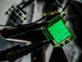
Carbon nanotubes bound for electronics need to be as clean as possible to maximize their utility in next-generation nanoscale devices, and scientists at Rice and Swansea universities have found a way to remove contaminants from the nanotubes.
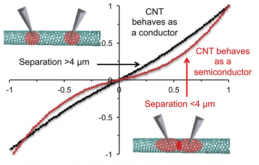
Scientists at Rice and Swansea universities have demonstrated that heating carbon nanotubes at high temperatures eliminates contaminants that make nanotubes difficult to test for conductivity. They found when measurements are taken within 4 microns of each other, regions of depleted conductivity caused by contaminants overlap, which scrambles the results. The plot shows the deviation when probes test conductivity from minus 1 to 1 volt at distances greater or less than 4 microns.
Barron Research Group/Rice University
Rice chemist Andrew Barron, also a professor at Swansea in the United Kingdom, and his team have figured out how to get nanotubes clean and in the process discovered why the electrical properties of nanotubes have historically been so difficult to measure.
Like any normal wire, semiconducting nanotubes are progressively more resistant to current along their length. But over the years, conductivity measurements of nanotubes have been anything but consistent. The Rice-Swansea team wanted to know why.
"We are interested in the creation of nanotube-based conductors, and while people have been able to make wires, their conduction has not met expectations," Barron said. "We wanted to determine the basic science behind the variability observed by other researchers."
They discovered that hard-to-remove contaminants -- leftover iron catalyst, carbon and water -- could easily skew the results of conductivity tests. Burning those contaminants away, Barron said, creates new possibilities for carbon nanotubes in nanoscale electronics.
The researchers first made multiwalled carbon nanotubes between 40 and 200 nanometers in diameter and up to 30 microns long. They then either heated the nanotubes in a vacuum or bombarded them with argon ions to clean their surfaces.
They tested individual nanotubes the same way one would test any electrical conductor: by touching them with two probes to see how much current passes through the material from one tip to the other. In this case, tungsten probes were attached to a scanning tunneling microscope.
In clean nanotubes, resistance got progressively stronger as the distance increased, as it should. But the results were skewed when the probes encountered surface contaminants, which increased the electric field strength at the tip. And when measurements were taken within 4 microns of each other, regions of depleted conductivity caused by contaminants overlapped, which further scrambled the results.
"We think this is why there's such inconsistency in the literature," Barron said. "If nanotubes are to be the next-generation lightweight conductor, then consistent results, batch-to-batch and sample-to-sample, are needed for devices such as motors and generators as well as power systems."
Heating the nanotubes in a vacuum above 200 degrees Celsius (392 degrees Fahrenheit) reduced surface contamination, but not enough to eliminate inconsistent results, they found. Argon ion bombardment also cleaned the tubes but led to an increase in defects that degrade conductivity.
Ultimately the researchers discovered vacuum annealing nanotubes at 500 degrees Celsius (932 Fahrenheit) reduced contamination enough to measure resistance accurately.
Barron said engineers who use nanotube fibers or films in devices currently modify the material through doping or other means to get the conductive properties they require. But if the source nanotubes are sufficiently decontaminated, they should be able to get the desired conductivity by simply putting their contacts in the right spot.
"A key result of our work is that if contacts on a nanotube are less than 1 micron apart, the electronic properties of the nanotube change from conductor to semiconductor, due to the presence of overlapping depletion zones, which shrink but are still present even in clean nanotubes," Barron said.
"This has a potential limiting factor on the size of nanotube-based electronic devices," he said. "Carbon-nanotube devices would be limited in how small they could become, so Moore's Law would only apply to a point."
Original publication
Other news from the department science


Get the chemical industry in your inbox
From now on, don't miss a thing: Our newsletter for the chemical industry, analytics, lab technology and process engineering brings you up to date every Tuesday and Thursday. The latest industry news, product highlights and innovations - compact and easy to understand in your inbox. Researched by us so you don't have to.