Nano-sandwich technique slims down solar cells, improves efficiency
Advertisement


Researchers from North Carolina State University have found a way to create much slimmer thin-film solar cells without sacrificing the cells' ability to absorb solar energy. Making the cells thinner should significantly decrease manufacturing costs for the technology.
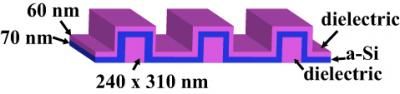
Researchers from North Carolina State University have found a way to create much slimmer thin-film solar cells without sacrificing the cells' ability to absorb solar energy. The active layer can be as little as 70 nanometers thick.
Dr. Linyou Cao, North Carolina State University
"We were able to create solar cells using a 'nanoscale sandwich' design with an ultra-thin 'active' layer," says Dr. Linyou Cao, an assistant professor of materials science and engineering at NC State and co-author of a paper describing the research. "For example, we created a solar cell with an active layer of amorphous silicon that is only 70 nanometers (nm) thick. This is a significant improvement, because typical thin-film solar cells currently on the market that also use amorphous silicon have active layers between 300 and 500 nm thick." The "active" layer in thin-film solar cells is the layer of material that actually absorbs solar energy for conversion into electricity or chemical fuel.
"The technique we've developed is very important because it can be generally applied to many other solar cell materials, such as cadmium telluride, copper indium gallium selenide, and organic materials," Cao adds.
The new technique relies largely on conventional manufacturing processes, but results in a very different finished product. The first step is to create a pattern on the substrate using standard lithography techniques. The pattern outlines structures made of transparent, dielectric material measuring between 200 and 300 nm. The researchers then coat the substrate and the nanostructures with an extremely thin layer of active material, such as amorphous silicon. This active layer is then coated with another layer of dielectric material.
Using dielectric nanostructures beneath the active layer creates a thin film with elevated surfaces evenly spaced all along the film – like crenellations at the top of a medieval castle.
"One key aspect of this technique is the design of the 'nanoscale sandwich,' with the active materials in the middle of two dielectric layers. The nanostructures act as very efficient optical antennas," Cao says, "focusing the solar energy into the active material. This focusing means we can use a thinner active layer without sacrificing performance. In the conventional thin-film design, using a thinner active layer would impair the solar cell's efficiency."
Original publication
Dielectric Core-shell Optical Antennas for Strong Solar Absorption Enhancement; Nano Letters


Other news from the department science


