Simulations for better transparent oxide layers
Touchscreens and solar cells rely on special oxide layers. However, errors in the layers’ atomic structure impair not only their transparency, but also their conductivity. Using atomic models, Fraunhofer researchers have found ways of identifying and removing these errors.
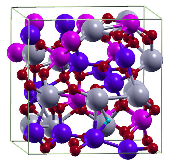
Detail from a model of an amorphous oxide layer into which hydrogen atoms have been introduced in a targeted process. The tiny light-blue sphere on the bottom right is hydrogen; oxygen is represented by small red spheres; the other spheres stand for indium (gray), tin (blue), and gallium (pink).
© Fraunhofer IWM
Smartphones, tablet computers, and ticket machines are just some of the many devices nowadays that are touchscreen-operated. These screens are based on special oxide layers that are transparent and conduct electricity. The technical term is TCO (transparent conducting oxide) layers. TCOs are also used on solar cells and in heated windows. So that the technology keeps pace with new products and applications, manufacturers are constantly improving the layers, making them better conductors of electricity and increasing their transparency – after all, when used in tablet computer or smartphone displays, users need to be able to see the content on the screen clearly through the layers. Any additional sheen caused by the oxide would be a problem. The same principle applies for solar cells: rather than impeding sunlight, the oxide layers must allow it to pass unobstructed into the cell. Accordingly, transparency and conductivity are the key elements that the developers of new oxide layers must consider – but the manufacturing temperature and the plasticity of the layers are also important.
Realistic simulation of atomic structure
Researchers at the Fraunhofer Institute for Mechanics of Materials IWM in Freiburg help manufacturers to optimize oxide layers. “We’ve developed a practical and effective method for simulating the properties of TCO layers,” says IWM scientist Dr. Wolfgang Körner. Most impressive of all is the fact that the scientists’ simulations of the layers’ atomic structure are highly realistic and take into account all possible atomic errors – irrespective of whether the layers are disordered, amorphous structures or crystalline, highly ordered ones. On the basis of these simulations, the scientists then investigate how well the electrons can move in the layer, in other words how well the oxide conducts electrical current. “We can specifically track how a layer’s density of states changes when we change its atomic structure,” explains Körner. The researchers can also establish whether light is absorbed or passes through the layer unobstructed, making it appear transparent. “Because we do the trial-and-error material tests on a computer, we can calculate the properties possessed by the respective material composition of the TCO being studied much faster and more cost-effectively than by traditional means,” says Körner. Through his projects, Körner is deepening our understanding of how the different properties of the oxide layers arise. This understanding is helping his industrial partners to improve their production and to obtain specific oxide layer properties.
The researchers have already managed to find the principal defects that occur in these layers. It is simply not possible to manufacture the structures with absolutely zero errors. As much as manufacturers want them to consist only of certain defined atoms such as zinc, tin, and oxygen, other atoms – hydrogen is a common culprit – have a habit of crashing the party, changing the layer’s conductivity and transparency. But what defects in atomic structure actually impair transparency? And how can we remove these defects to make the oxides more transparent? One of the researchers’ findings was that the transparency of certain oxides is improved by heating them once to a suitably high temperature or by heating them up in an oxygen-rich environment.
A second approach sees the scientists tackle the problem from the other end: they add various specifically defined atoms into the structure and simulate the effects this has on a layer’s properties. The goal here is to further boost conductivity and transparency by means of suitable “impurities” and to be able to design a material by computer in this way.
Other news from the department science


Get the chemical industry in your inbox
From now on, don't miss a thing: Our newsletter for the chemical industry, analytics, lab technology and process engineering brings you up to date every Tuesday and Thursday. The latest industry news, product highlights and innovations - compact and easy to understand in your inbox. Researched by us so you don't have to.