Graphene plasmons go ballistic
Graphene combined with the insulting power of boron nitride enables light control in tiny circuits with dramatically reduced energy loss
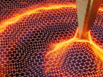
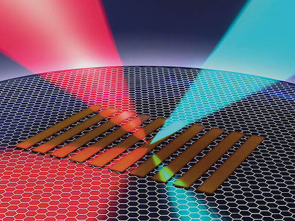
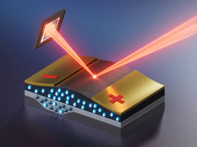
Squeezing light into tiny circuits and controlling its flow electrically is a holy grail that has become a realistic scenario thanks to the discovery of graphene. This tantalizing achievement is realized by exploiting so-called plasmons, in which electrons and light move together as one coherent wave. Plasmons guided by graphene - a two-dimensional sheet of carbon atoms - are remarkable as they can be confined to length scales of nanometers, up to two hundred times below the wavelength of light. An important hurdle until now has been the rapid loss of energy that these plasmons experience, limiting the range over which they could travel.
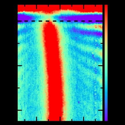
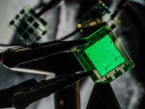
This image shows simulation and observations of propagating plasmons in boron nitride heterostructure.
ICFO
This problem has now been solved, as shown by researchers from ICFO (Barcelona), in a collaboration with CIC nanoGUNE (San Sebastian), and CNR/Scuola Normale Superiore (Pisa) ,all members of the EU Graphene Flagship, and Columbia University (New York).
Since the discovery of graphene, many other two-dimensional materials have been isolated in the laboratory. One example is boron nitride, a very good insulator. A combination of these two unique two-dimensional materials has provided the solution to the quest for controlling light in tiny circuits and suppression of losses. When graphene is encapsulated in boron nitride, electrons can move ballistically for long distances without scattering, even at room temperature. This research now shows that the graphene/boron nitride material system is also an excellent host for extremely strongly confined light and suppression of plasmon losses.
ICFO Prof Frank Koppens comments that "it is remarkable that we make light move more than 150 times slower than the speed of light, and at lengthscales more than 150 times smaller than the wavelength of light. In combination with the all-electrical capability to control nanoscale optical circuits, one can envision very exciting opportunities for applications."
The research, carried out by PhD students Achim Woessner (ICFO) and Yuando Gao (Columbia) and postdoctoral fellow Mark Lundeberg (ICFO), is just the beginning of a series of discoveries on nano-optoelectronic properties of new heterostructures based on combining different kinds of two-dimensional materials. The material heterostructure was first discovered by the researchers at Columbia University. Prof. James Hone comments: "Boron nitride has proven to be the ideal 'partner' for graphene, and this amazing combination of materials continues to surprise us with its outstanding performance in many areas".
Prof. Rainer Hillenbrand from CIC nanoGUNE comments: "Now we can squeeze light and at the same time make it propagate over significant distances through nanoscale materials. In the future, low-loss graphene plasmons could make signal processing and computing much faster, and optical sensing more efficient."
The research team also performed theoretical studies. Marco Polini, from CNR/Scuola Normale Superiore (Pisa) and the IIT Graphene Labs (Genova), laid down a theory and performed calculations together with his collaborators. He explains that "according to theory, the interactions between light, electrons and the material system are now very well understood, even at a fully microscopic level. It is very rare to find a material that is so clean and in which this level of understanding is possible".
These findings pave the way for extremely miniaturized optical circuits and devices that could be useful for optical and/or biological sensing, information processing or data communications.
Original publication
Other news from the department science


Get the chemical industry in your inbox
From now on, don't miss a thing: Our newsletter for the chemical industry, analytics, lab technology and process engineering brings you up to date every Tuesday and Thursday. The latest industry news, product highlights and innovations - compact and easy to understand in your inbox. Researched by us so you don't have to.