A different type of 2-D semiconductor
To the growing list of two-dimensional semiconductors, such as graphene, boron nitride, and molybdenum disulfide, whose unique electronic properties make them potential successors to silicon in future devices, you can now add hybrid organic-inorganic perovskites. However, unlike the other contenders, which are covalent semiconductors, these 2D hybrid perovskites are ionic materials, which gives them special properties of their own.
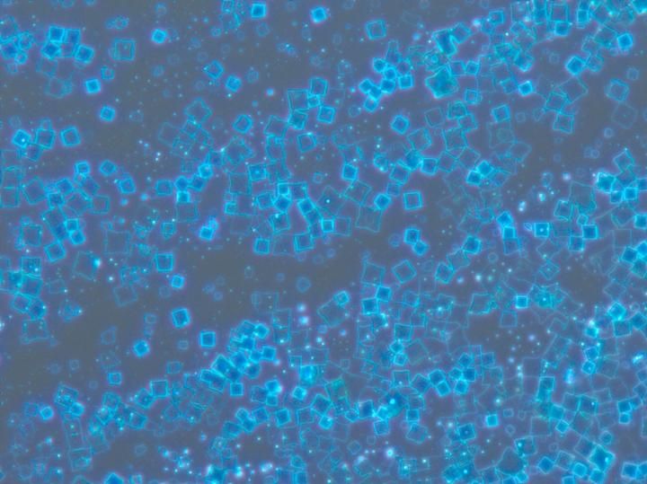
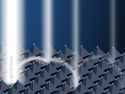
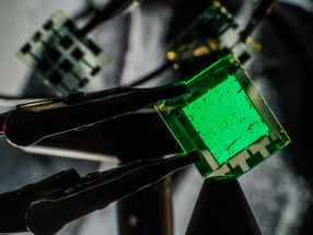
Ultrathin sheets of a new 2-D hybrid perovskite are square-shaped and relatively large in area, properties that should facilitate their integration into future electronic devices.
Peidong Yang, Berkeley Lab
Researchers at the Lawrence Berkeley National Laboratory have successfully grown atomically thin 2D sheets of organic-inorganic hybrid perovskites from solution. The ultrathin sheets are of high quality, large in area, and square-shaped. They also exhibited efficient photoluminescence, color-tunability, and a unique structural relaxation not found in covalent semiconductor sheets.
"We believe this is the first example of 2D atomically thin nanostructures made from ionic materials," says Peidong Yang, a chemist with Berkeley Lab's Materials Sciences Division and world authority on nanostructures, who first came up with the idea for this research some 20 years ago. "The results of our study open up opportunities for fundamental research on the synthesis and characterization of atomically thin 2D hybrid perovskites and introduces a new family of 2D solution-processed semiconductors for nanoscale optoelectronic devices, such as field effect transistors and photodetectors."
While a PhD student at Harvard University, Yang proposed a method for preparing 2D hybrid perovskite nanostructures and tuning their electronic properties but never acted upon it. This past year, while preparing to move his office, he came upon the proposal and passed it on to co-lead author Dou, a post-doctoral student in his research group. Dou, working mainly with the other lead authors Wong and Yu, used Yang's proposal to synthesize free-standing 2D sheets of a hybrid perovskite.
"Unlike exfoliation and chemical vapor deposition methods, which normally produce relatively thick perovskite plates, we were able to grow uniform square-shaped 2D crystals on a flat substrate with high yield and excellent reproducibility," says Dou. "We characterized the structure and composition of individual 2D crystals using a variety of techniques and found they have a slightly shifted band-edge emission that could be attributed to structural relaxation. A preliminary photoluminescence study indicates a band-edge emission at 453 nanometers, which is red-shifted slightly as compared to bulk crystals. This suggests that color-tuning could be achieved in these 2D hybrid perovskites by changing sheet thickness as well as composition via the synthesis of related materials."
The well-defined geometry of these square-shaped 2D crystals is the mark of high quality crystallinity, and their large size should facilitate their integration into future devices.
"With our technique, vertical and lateral heterostructures can also be achieved," Yang says. "This opens up new possibilities for the design of materials/devices on an atomic/molecular scale with distinctive new properties."
Original publication
Other news from the department science


Get the chemical industry in your inbox
From now on, don't miss a thing: Our newsletter for the chemical industry, analytics, lab technology and process engineering brings you up to date every Tuesday and Thursday. The latest industry news, product highlights and innovations - compact and easy to understand in your inbox. Researched by us so you don't have to.