Surprise at the nanoscale: Silicon atoms jump after contact with metal
Max Planck researchers reveal unknown behaviour of semi-conductors at the nanoscale
silicon is presently the most proper ingredient for microelectronic devices: it serves as basic material for all current computer chips. According to the increasing importance of electronic set-ups, the term “Silicon Age” is widely-used nowadays.
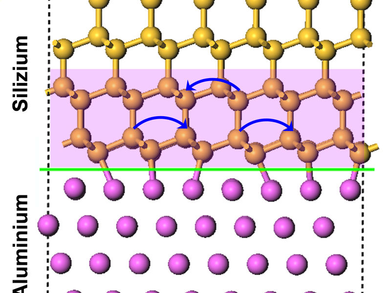
Semiconductor atoms (as silicon and germanium atoms) get influenced by metal (as aluminium) at the nanoscale and change their position through atomic jumps, even at temperatures as low as -190 degree celsius.
© Dr. Zumin Wang, MPI-IS Stuttgart
Further, the nickname Silicon Valley, representing the high-tech region in California, indicates the enormous importance of silicon for the semi-conductor and computer industry.
Crystalline silicon has also been widely used for the production of TFT-flatscreens and is, furthermore, a fundamental basic material for the assembling of photovoltaic cells.
A further semiconductor is germanium, which initially was the leading material in (micro) electronics, until it was replaced by silicon. Only few years ago, researchers discovered that monolayers of germanium conduct electrons up to 10 times faster than silicon. For this reason, germanium could catch up as semi-conductor again.
Silicon and germanium are both quite heat resistant and melt only at temperatures higher than 900 degree Celsius. At the solid state, the atoms are positioned within a regularly ordered crystal lattice and can only vibrate slightly at their respective locations. With increasing temperature, the vibrations intensify and even “jumps“ to different sites in the solid occur. At room temperature these kind of atomic jumps are practically impossible.
Scientists led by Prof. Dr. Ir. Eric Jan Mittemeijer, Director at the Max Planck Institute for Intelligent Systems in Stuttgart, have recently discovered that atomic jumps occur in silicon and germanium even at very low temperature of minus 190 degree Celsius, if the thin layer of only 1 nanometer (millionth millimeter) gets in contact with metal, e.g. aluminium.
The researcher Dr. Zumin Wang reports: „We tried to prepare artificial sandwiches composed of a very thin, 1-nm silicon or germanium film between two aluminium layers at minus 190 degree celsius. During this process we figured out that germanium or silicon always moved to the top surface of the aluminium. It was not possible to prepare such sandwiches. First, we found this “behavior” quite annoying, but soon we recognized that we had made a very surprising observation.”
While using X-ray photoelectron spectroscopy, the scientists found out that the bonding characteristics within germanium- and silicon atoms become strongly influenced when they get in touch with metals at thin-film set-ups. As a consequence, the semi-conductor atoms become able to “jump” more frequently. Because of these jumps, the atoms get mobile and change their position: they jump to the top surface of the aluminium. The metal influences this mobility and has to be as close as half a nanometer.
Dr. Wang states: “This observation could become even more important since assembly parts for computers made of semi-conductor material shrink increasingly. Currently they are already as small as 10 to 40 nanometer, which means that at slightly smaller scale, mixing effects due to atomic jumps may arise. Secondly, the discovered process has impact on the preparation of thin film systems involving heat-sensitive materials, since the semi-conductor can become mobile even at very low temperature.”
Original publication
Zumin Wang, Lars P. H. Jeurgens, Wilfried Sigle, and Eric J. Mittemeijer; “Observation and Origin of Extraordinary Atomic Mobility at Metal-Semiconductor Interfaces at Low Temperatures”; Physical Review Letters 115, 016102 (2015).
Other news from the department science


Get the chemical industry in your inbox
From now on, don't miss a thing: Our newsletter for the chemical industry, analytics, lab technology and process engineering brings you up to date every Tuesday and Thursday. The latest industry news, product highlights and innovations - compact and easy to understand in your inbox. Researched by us so you don't have to.
Most read news


More news from our other portals


See the theme worlds for related content
Topic World Spectroscopy
Investigation with spectroscopy gives us unique insights into the composition and structure of materials. From UV-Vis spectroscopy to infrared and Raman spectroscopy to fluorescence and atomic absorption spectroscopy, spectroscopy offers us a wide range of analytical techniques to precisely characterize substances. Immerse yourself in the fascinating world of spectroscopy!