Successful real-time observation of atomic motion with sub-nanometer resolution
Associate Professor Muneaki Hase of the Faculty of Pure and Applied Sciences of the University of Tsukuba, Dr. Paul Fons, Chief Researcher in the Nanoelectronics Division of the National Institute of Advanced Industrial Science and Technology, Lecturer Toru Shimada of Hirosaki University, Dr. Makina Yabashi, group director of the Beam Line Research and Development Group at the Riken SPring-8 Center, and Drs. Tadashi Togashi and Tetsuo Katayama of the Japan synchrotron radiation Institute have succeeded in using the immensely powerful x-ray pulses from the free electron laser (XFEL) facility SACLA *1 to investigate excited-state induced transient lattice dynamics on sub-picosecond time scales in phase-change materials via x-ray diffraction. Phase-change materials (PCM) are broadly used in the current generation of rewritable DVD media*2 as well as serving as the basis for nonvolatile phase-change random access memory (PC-RAM)*3 widely believed to the successor to FLASH memory. The XFEL SACLA produces extremely bright and short intense (10 fs) pulses in the x-ray region and is the first domestic X-ray laser source in Japan. The ultrashort nature of the x-ray pulses in conjunction with their short wavelength (10-10 m) allow direct stroboscopic observation of transient changes in the atomic structure of solids on unprecedented time scales.
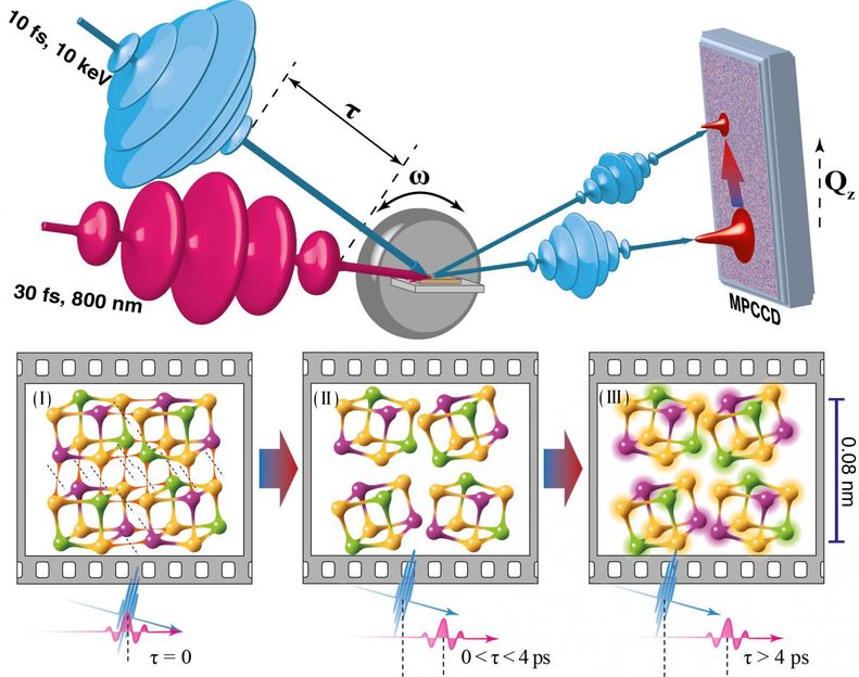
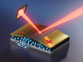
(upper) A schematic representation of the pump-probe time-resolved x-ray diffraction technique. After irradiation of the sample by a near-infrared excitation pulse (red color), an XFEL pulse (blue) delayed by a time τ irradiates the sample and the resulting changes in the diffraction peak intensity and position are recorded by the multi-port CCD (MPCCD). ω represents the rotation of the sample. (lower) Frames (I) to (III) show schematic changes in the Ge2Sb2Te5 single crystal induced by the femosecond excitation. Ge atoms are shown in yellow, Te atoms in blue, and Sb atoms are shown in purple.
University of Tsukuba
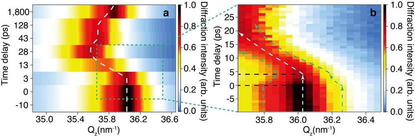
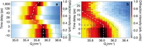
Time-resolved changes in (222) plane x-ray diffraction signal. (a) Changes in the x-ray diffraction peak from -10 to +1800 ps are shown. The horizontal axis is a wavenumber. (b) Changes in the x-ray diffraction peak from -10 to +30 ps are shown in magnified form. Before optical excitation, the diffraction peak is located at about 36 nm-1, while immediately after excitation the intensity begins to decrease and after a delay of about 4 ps, the peak starts to shift to smaller wavenumber. The shift reaches a maximum value for about a 20 ps delay. After about 1.8 ns, the peak reverts to its original position.
University of Tsukuba
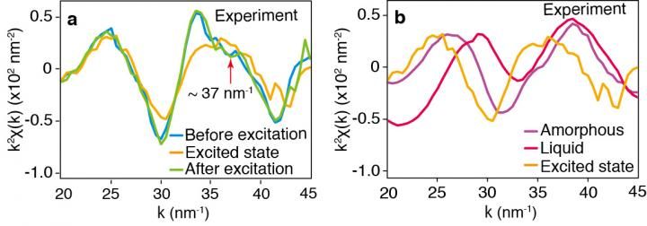
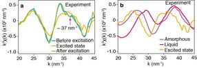
Time-resolved x-ray absorption spectroscopy (XAFS) structural measurements of a polycrystalline film of Ge2Sb2Te5. (a) With electrons excited by an ultrafast laser pulse (excited state), before excitation, and after excitation. (b) Reference spectra for the amorphous state and the liquid state compared with the excited state spectra.
University of Tsukuba
In the research project, an ultrafast pulsed laser*4 was used to optically excite a Ge2Sb2Te5 epitaxially film and x-ray pulses from the XFEL were used to record the subsequent transient changes in atomic positions in the newly created excited state with sub-picosecond precision using x-ray diffraction. These observations revealed that immediately after excitation, bond breaking induced by the excited state resulted in non-thermal local structural rearrangements within a few picoseconds followed by warming of the lattice after 4 picoseconds. The formation of the heretofore unobserved transient structural state was followed by a 2 picometer (= 10-12 m) change in lattice spacing after 20 picoseconds as revealed by x-ray diffraction. The transient state was observed to persist for over 100 picoseconds, but was found to complete revert to the initial (ground) state after 1.8 nanoseconds.
The presence of this previously unknown transient state formed on picosecond time scales strongly suggests that the usual thermally-induced nanosecond order transition of conventional phase-change memory may be used to speed up memory switching to picosecond time scales. In other words, the use of electronic excitation in the phase-change transition process is expected to enable picosecond time-scale memory operation.
Background and details of the research
Upon irradiation of a solid by a laser pulse, electrons are excited from the ground state to higher levels leading to the creation of an excited state*5 in the solid. A solid in such an excited state is said to be in a metastable or unstable state and typically atoms are displaced from their equilibrium positions in the ground state. By intentionally creating an excited state in a solid, it is possible to induce displacements in atomic positions allowing manipulation of the crystal structure of the solid. The displacements in atomic positions induced by such processes, however, are typically on the sub-nanometer (0.1 nm) scale making it impossible to assess such small changes using laser light with a wavelength of several hundred nanometers. To measure such small changes in position, it is necessary to use sub-nanometer wavelength light from the x-ray laser in the form of time-resolved x-ray diffraction.
Optical recording materials such as those used for DVD-RAM are semiconducting chalcogen compounds largely composed of Te and the class of such compounds is often referred to as phase-change materials. Phase-change materials exhibit large changes in material properties such as optical reflectivity and electrical resistance between crystalline and amorphous states making them useful for recording information based upon the corresponding property changes. To date, the typical time for recording of information using these two states has been on the order of a nanosecond (one billionth of a second). In recent years, however, first-principles calculations*6 have predicted that by use of electronic excitation, such transitions can be made to occur on picosecond time scales (one trillionth of a second)a. If these predictions are realized, major strides in both low power operation and data throughput will be achievable using nonvolatile phase-change memory.
To advance these goals, the current research team used the world's most advanced free-electron x-ray laser facility [SACLA] to carry out time-resolved x-ray diffraction measurements of the atomic motion in a phase-change material on sub-nanometer spatial scales.
Research Contents and Results
In the framework of the research project Ge2Sb2Te5 epitaxial thin films (thickness 35 nm) were fabricated and irradiated with ultrashort duration (30 femtoseconds) laser light (wavelength 800 nm) at SACLA. This resulted in the optical excitation of electrons in the Ge2Sb2Te5 film and the creation of an excited state in the sample. In order to capture the resulting atomic motion after excitation, XFEL pulses (10 femtoseconds duration with 10 keV energy) were used to stroboscopically observe changes in the sample structure using a multiple port readout CCD (MPCCD) detector to record x-ray diffraction images at thirty frames a second. For the current experiments, x-ray diffraction from the epitaxially grown, highly perfect single crystal sample resulted in peak-based diffraction images being recorded by the MPCCD as is schematically shown. The highest intensity diffraction plane (222) was chosen as the subject of the time-resolved diffraction experiments and changes in both the location and intensity of the x-ray diffraction peaks were tracked with sub-picosecond time resolution. In this way, the changes in the positions of the atoms constituting the Ge2Sb2Te5 single crystal could be followed on the ultrafast sub-picosecond time scale of the present experiment.
Using the above technique, the displacement of atoms from the crystal equilibrium position were found to reach a maximum at about 20 picoseconds resulting in a maximum diffraction peak shift (0.45 nm-1) with a corresponding atomic displacement of about 2 picometer. Subsequently after about 1.8 nanoseconds, the atom positions were found to revert to those of the perfect crystal. Changes in the positions of the x-ray diffraction peaks on the MPCCD reflect the changes in the lattice spacing of the crystal while reductions in the intensity of the peaks reflect changes in the magnitude of mean square vibrations of the atoms about their average positions (Debye-Waller Effect *7). The changes are schematically indicated where the initial lattice softening resulting from bond breaking and local atomic rearrangements induced by the electrons excitation, even though the lattice remains at room temperature (the second frame (II)). Subsequent to this, the temperature of the lattice rises and leads to further expansion of the lattice plane spacing (frame III). Thus, a 2 picometer atomic displacement was induced as the transition from frame (II) to frame (III).
The current measurements as visualized allowed observation of extremely small changes, less than about 0.08 nm. In addition, the same excitation-induced changes that occurred in less than 1.8 nanoseconds were studied at the Advanced Photon Source*8 using x-ray absorption spectroscopy to understand the microscopic details of the transition from the crystalline to the amorphous state.
Future Developments
The current research has investigated the details of the phase change process in both rewritable optical and nonvolatile memory phase-change materials on picosecond time scales. Also recently it was found that similar sub-picosecond processes occur in thin film GeTe/Sb2Te3 superlattices*9 leadingb to the promise of future generations of phase-change material based devices working at unprecedented speeds and lower power operation than the current generation of Ge2Sb2Te5 alloy films.
Furthermore, it was demonstrated that the sub-nanometer, sub-picosecond time scale processes can be observed using time-resolved x-ray diffraction at SACLA. In future developments, it is anticipated that time resolved diffraction measurements will be carried out with a time resolution better than 100 femtoseconds allowing for the measurement and understanding of transition dynamics of a wide range of materials.
Original publication
Kirill V. Mitrofanov, Paul Fons, Kotaro Makino, Ryo Terashima, Toru Shimada, Alexander V. Kolobov, Junji Tominaga, Valeria Bragaglia, Alessandro Giussani, Raffaella Calarco, Henning Riechert, Takahiro Sato, Tetsuo Katayama, Kanade Ogawa, Tadashi Togashi, Makina Yabashi, Simon Wall, Dale Brewe & Muneaki Hase; "Sub-nanometre resolution of atomic motion during electronic excitation in phase-change materials"; Scientific Reports; 2016
Other news from the department science


Get the chemical industry in your inbox
From now on, don't miss a thing: Our newsletter for the chemical industry, analytics, lab technology and process engineering brings you up to date every Tuesday and Thursday. The latest industry news, product highlights and innovations - compact and easy to understand in your inbox. Researched by us so you don't have to.