Bath semiconductor research boosted by new nano-scale patterning equipment
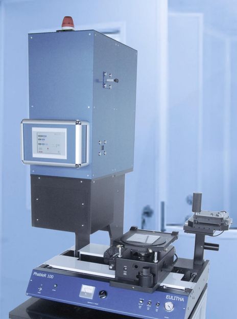
The University of Bath is the only university in the UK to have installed a unique Nano-lithography printing system, enabling Bath to lead the way in the development of advanced manufacturing techniques for nano-engineered semiconductors.

Researchers at Bath will use the new Nano-Lithography printing system to accelerate its research into nano-engineered LEDs.
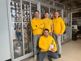
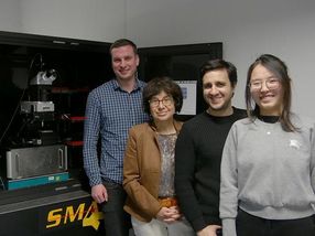
University of Bath
The University of Bath is the only university in the UK to have this innovative nano-scale patterning equipment.
University of Bath


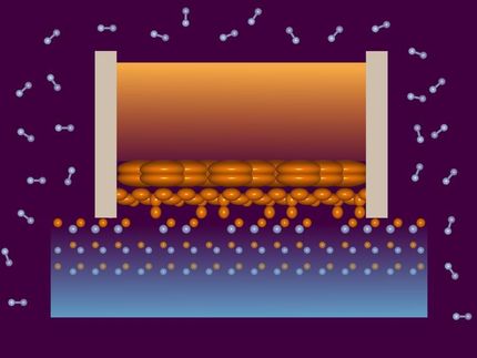
Based in the University's Department of Electronic & Electrical Engineering, the PhableR 100 Nano-Lithography System is capable of printing very high resolution periodic patterns at a low-cost meaning new electronic devices that exploit the properties of nano-scale features can be more easily scaled up for production.
Such devices have been the focus of extensive research for over a decade and this new equipment will help Bath to contribute in ensuring these developments are translated into products in the market.
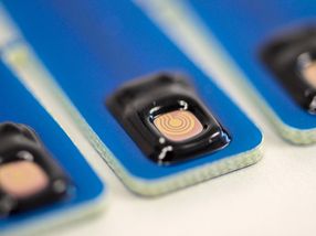
The III-nitride research group at the University of Bath has been using nanolithography for several years in its research to improve the efficiency and reduce the cost of the light-emitting diodes (LEDs) used for general lighting. The semiconductor Gallium Nitride (GaN) is key to this technology and the research group will use the new system to accelerate its research into nano-engineered LEDs.
Creating three-dimensional structures at the nanoscale provides a route to improving the quality of these materials and in turn the performance of these devices. Ultimately this will increase the energy efficiency in these and other emerging applications, such as water purification, where ultra-violet LEDs are used to prevent viruses reproducing.
This innovative system was purchased following a £2.7 million Engineering & Physical Sciences Research Council (EPSRC) grant as part of the council's Manufacturing of Advanced Functional Materials funding programme.
Lead researcher and Lecturer in the Department of Electronic and Electrical Engineering, Dr Philip Shields, said: "We are very excited to have this new capability at Bath. Initial results from the tool have matched and even exceeded our expectations. There has been a lot of interest from other researchers to use the tool and we look forward to developing new research collaborations as a consequence."
Dr Harun Solak, CEO of Eulitha, said: "We are very pleased to have supplied the University of Bath with this equipment. Their research program focuses on manufacturing technologies for nano-engineered semiconductors which is an area where our innovative technologies have the potential to make a significant impact."
Only two other universities in the world have acquired this revolutionary Eulitha equipment, Twente University in the Netherlands and CIOMP Institute in China.
Head of the Department of Electronic and Electrical Engineering, Dr Adrian Evans added: "The installation of this system will produce a step change in the Department's advanced nano-manufacturing techniques. It is significant that this is the only system of its type in the UK and will further enhance Bath's research and impact in this exciting area."

Other news from the department science


Get the chemical industry in your inbox
From now on, don't miss a thing: Our newsletter for the chemical industry, analytics, lab technology and process engineering brings you up to date every Tuesday and Thursday. The latest industry news, product highlights and innovations - compact and easy to understand in your inbox. Researched by us so you don't have to.