Lasers on silicon
Low temperature heterogeneous integration without glue
Realization of large scale photonic integration for one-chip optical routers is crucial for future optical networks and interconnection for big data transmission and artificial intelligence technology. To meet these technical needs, platforms based on silicon photonic integrated circuits are expected to play an important role because of the availability of large diameter wafers and CMOS fabrication technology.
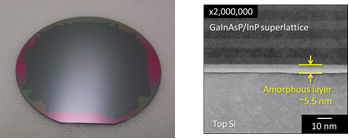
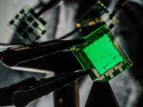
Optical microscope and SEM images of GaInAsP/SOI hybrid wafers.
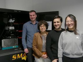
Arai Lab, Tokio Tech
However, it is difficult to realize light sources using silicon because it is an indirect bandgap semiconductor.
Now, Nobuhiko Nishiyama and colleagues at Tokyo Institute of Technology have demonstrated the operation of 1.55-μm GaInAsP lasers on silicon using low temperature plasma activated bonding (PAB).
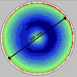
The hybrid wafers, which consist of an InP-based wafer and a SOI wafer, were fabricated by PAB. The two wafers were irradiated with plasma in a vacuum chamber to active the surface. Then, the two wafers were bonded at 150 oC, which is much lower than that of conventional bonding methods. Even at such low temperature bonding, the wafers had sufficient bonding strength.
The hybrid lasers showed lasing operation at room temperature. The threshold current was 64 mA, which corresponds to a threshold current density of 850 A/cm2.
These hybrid lasers fabricated by low temperature bonding are expected to be a key technology to establish large scale photonic platforms.
Original publication
Other news from the department science


Get the chemical industry in your inbox
From now on, don't miss a thing: Our newsletter for the chemical industry, analytics, lab technology and process engineering brings you up to date every Tuesday and Thursday. The latest industry news, product highlights and innovations - compact and easy to understand in your inbox. Researched by us so you don't have to.