Towards future lab-on-chip applications
Fraunhofer FEP presents latest approaches to fabricate OLED devices for lab-on-a-chip-applications using either near UV electroluminescence (EL) or optically modulated green light to stimulate fluorescent dye markers.
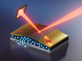
Smart and portable medical equipment is essential for fast and easy point-of-care and point-of-use diagnostics. Lab-on-a-chip applications in hand-held devices can help to save time for laboratory medical analysis in emergency scenarios. The combination of sub-micrometer-thick light emitting devices and photo-detectors with tunable spectral characteristics could play a key role in future sensing chips based on organic electronics.
These applications realize the excitation and detection of fluorescence or phosphorescence in a marker. Even time-resolved measurements are possible. The integration of both, OLED together with organic photodiodes into one chip could be a way to achieve low-cost personal diagnostics outside the laboratory.
At IDW 2014 Fraunhofer FEP presents two different OLED-device concepts: one emitting in the near UV and another one in the green spectral range which both could be integrated to sensor applications.
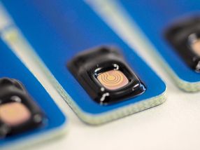
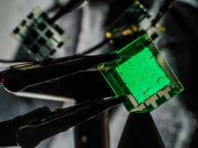
These two exemplary OLED developments can be used for biomedical and biotechnical sensing in lab-on-chip applications. Near ultra-violet emission from an OLED is demonstrated for bottom- as well as from top-emitting device architectures. Furthermore, the scientists from Fraunhofer FEP combined a green top-emitting OLED with a thin-film optical filter and thin-film encapsulation so that a sample substance can be brought in proximity to the excitation source. Both developed devices are suitable for large area deposition and integration on silicon-backplanes like wafers as light source for optical excitation to detect fluorescence or phosphorescence signals.
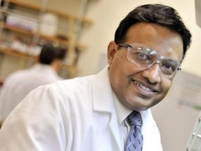
Dr. Michael Thomschke, project leader at Fraunhofer FEP states: “These developments could be incorporated in very small ultra-thin organic devices based on glass, foil or opaque silicon-backplanes. The integration e.g. on silicon-wafers could be very cost-efficient. The corresponding processes allow large area manufacturing as well as devices in the µm scale.”
Later on, such device could be extended with microfluidics or external optics to fit a certain application.
Other news from the department science


Get the chemical industry in your inbox
From now on, don't miss a thing: Our newsletter for the chemical industry, analytics, lab technology and process engineering brings you up to date every Tuesday and Thursday. The latest industry news, product highlights and innovations - compact and easy to understand in your inbox. Researched by us so you don't have to.