To use all functions of this page, please activate cookies in your browser.
My watch list
my.chemeurope.com
my.chemeurope.com
With an accout for my.chemeurope.com you can always see everything at a glance – and you can configure your own website and individual newsletter.
- My watch list
- My saved searches
- My saved topics
- My newsletter
Active pixel sensorAn active-pixel sensor (APS), also commonly written active pixel sensor, is an image sensor consisting of an integrated circuit containing an array of pixel sensors, each containing a photodetector and connecting to an active transistor reset and readout circuit. Such an image sensor is produced by a CMOS process (and is hence also known as a CMOS sensor), and has emerged as an inexpensive alternative to charge-coupled device (CCD) imagers. The term active pixel sensor is also used to refer to the individual pixel sensor itself, as opposed to the image sensor;[1] in that case the image sensor is sometimes called an active pixel sensor imager,[2] active-pixel image sensor,[3] or active-pixel-sensor (APS) imager. Product highlight
HistoryThe active-pixel sensor is descended from the original MOS active-pixel image sensors, which, like the CCD, were invented in the late 1960s. Noble in 1968[4] and Chamberlain in 1969[5] created sensor arrays with active MOS readout amplifiers per pixel, in essentially the modern three-transistor configuration. Other early MOS image sensors, at about the same time, were passive-pixel sensors; each passive pixel contained a photodiode and an access transistor.[6] Pixels were arrayed in a two-dimensional structure, with access enable wire shared by pixels in the same row, and output wire shared by column. At the end of each column was an amplifier. Passive-pixel sensors suffered from many limitations, such as high noise, slow readout, and lack of scalability. The addition of an amplifier to each pixel addressed these problems, and resulted in the creation of the active-pixel sensor. Similar devices to the APS concept were in production as early as 1978 for use in Infrared Focal-Plane Arrays (IRFPA). Although these devices were CMOS/InGaAs or HgCdTe hybrids, the key difference from the later CMOS devices was that the photodiodes were not integrated into the readout substrate. In 1992, Eric Fossum, et al., published the first extensive article[7] predicting the emergence of APS sensors as the commercial successor of CCDs. Between 1993 and 1995, the Jet Propulsion Laboratory developed a number of prototype devices which validated the key features of the technology. Though primitive, these devices demonstrated good image performance with high readout speed and low power consumption. In 1995, personnel from JPL founded Photobit Corp., who continued to develop and commercialize APS technology for a number of applications, such as web cams, digital radiography, and endoscopy cameras. Comparison to CCDs
The APS pixel solves the speed and scalability issues of the passive-pixel sensor. They consume far less power than a CCD, have less image lag, and can be fabricated on much cheaper and more available manufacturing lines. Unlike CCDs, APS sensors can combine both the image sensor function and image processing functions within the same integrated circuit. APS imagers still suffer from higher fixed pattern noise than CCDs, but active pixel sensors are catching up with respect to noise, dynamic range, and responsivity. APS sensors have become the technology of choice for many consumer applications, most significantly, the burgeoning cell phone camera market. However, adoption of APS image sensors has also found inroads in many other growing fields of photography and imaging. These include digital radiography, military ultra high speed image acquisition, high resolution 'smart' security cameras, as well as many other consumer applications. A number of semiconductor manufacturers offer APS sensors of various types. These include Micron Technology (who purchased Photobit in 2001), Samsung, ST Micro, Toshiba, Omnivision Technology, MagnaChip, Sony, and Canon, among others. Architecture
PixelThe standard CMOS APS pixel consists of three transistors as well as a photodetector. The photodetector is usually a photodiode, though photogate detectors are used in some devices and can offer lower noise through the use of correlated double sampling. Light causes an accumulation, or integration of charge on the 'parasitic' capacitance of the photodiode, creating a voltage change related to the incident light. One transistor, Mrst, acts as a switch to reset the device. When this transistor is turned on, the photodiode is effectively connected to the power supply, VRST, clearing all integrated charge. Since the reset transistor is n-type, the pixel operates in soft reset. The second transistor, Msf, acts as a buffer (specifically, a source follower), an amplifier which allows the pixel voltage to be observed without removing the accumulated charge. Its power supply, VDD, is typically tied to the power supply of the reset transistor. The third transistor, Msel, is the row-select transistor. It is a switch that allows a single row of the pixel array to be read by the read-out electronics. Other innovations of the pixels such as 4T, 5T and 6T pixels also existed. By adding extra transistor as in 4T pixel, such as transfer gate is added between the photodiode and floating diffusion enable the correlated double sampling. In order to increase the pixel densities, shared-row, 4-ways shared and eight-ways shared read out architertures can be employed. ArrayA typical two-dimensional array of pixels is organized into rows and columns. Pixels in a given row share reset lines, so that a whole row is reset at a time. The row select lines of each pixel in a row are tied together as well. The outputs of each pixel in any given column are tied together. Since only one row is selected at a given time, no competition for the output line occurs. Further amplifier circuitry is typically on a column basis. Design variants
Many different pixel designs have been proposed and fabricated. The standard pixel is the most common because it uses the fewest wires and the fewest, most tightly-packed transistors possible for an active pixel. It is important that the active circuitry in a pixel take up as little space as possible to allow more room for the photodetector. High transistor count hurts fill factor, that is, the percentage of the pixel area that is sensitive to light. Pixel size can be traded for desirable qualities such as noise reduction or reduced image lag. Noise is a measure of the accuracy with which the incident light can be measured. Lag occurs when traces of a previous frame remain in future frames, i.e. the pixel is not fully reset. The voltage noise variance in a soft-reset (gate-voltage regulated) pixel is Hard resetOperating the pixel in hard reset increases noise ( Another way to achieve hard reset, with the n-type FET, is to lower the voltage of VRST relative to the on-voltage of RST. This reduction may reduce headroom, or full-well charge capacity, but does not affect fill factor, unless VDD is then routed on a separate wire with its original voltage.. Combinations of hard and soft resetTechniques such as flushed reset, pseudo-flash reset, and hard-to-soft reset combine soft and hard reset. The details of these methods differ, but the basic idea is the same. First, a hard reset is done, eliminating image lag. Next, a soft reset is done, causing a low noise reset without adding any lag. Pseudo-flash reset requires separating VRST from VDD, while the other two techniquies add more complicated column circuitry. Specifically, pseudo-flash reset and hard-to-soft reset both add transistors between the pixel power supplies and the actual VDD. The result is lower headroom, without affecting fill factor. Active resetA more radical pixel design is the active-reset pixel. Active reset can result in much lower noise levels. The tradeoff is a complicated reset scheme, as well as either a much larger pixel or extra column-level circuitry. References
Further reading
|
|||||||
| This article is licensed under the GNU Free Documentation License. It uses material from the Wikipedia article "Active_pixel_sensor". A list of authors is available in Wikipedia. |


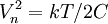 , but image lag and fixed pattern noise may be problematic. In rms electrons, the noise is
 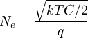 .
.
 ,
,  ), but removes lag, sometimes a desirable tradeoff. One way to use hard reset is replace Mrst with a p-type transistor and invert the polarity of the RST signal. The presence of the p-type device reduces fill factor, as extra space is required between p- and n-devices; it also removes the possibility of using the reset transistor as an overflow anti-blooming drain, which is a commonly-exploited benefit of the n-type reset FET.


