To use all functions of this page, please activate cookies in your browser.
My watch list
my.chemeurope.com
my.chemeurope.com
With an accout for my.chemeurope.com you can always see everything at a glance – and you can configure your own website and individual newsletter.
- My watch list
- My saved searches
- My saved topics
- My newsletter
MicrostripMicrostrip is a type of electrical transmission line which can be fabricated using printed circuit board [PCB] technology, and is used to convey microwave-frequency signals. It consists of a conducting strip separated from a ground plane by a dielectric layer known as the substrate. Microwave components such as antennas, couplers, filters, power dividers etc. can be formed from microstrip, the entire device existing as the pattern of metallization on the substrate. Microstrip is thus far cheaper than traditional waveguide technology, as well as being far lighter and more compact. The disadvantages of microstrip compared with waveguide are the generally lower power handling capacity, and higher losses. Also, unlike waveguide, microstrip is not enclosed, and is therefore susceptible to cross-talk and unintentional radiation. For lowest cost, microstrip devices may be built on an ordinary FR4 (standard PCB) substrate. However it is often found that the dielectric losses in FR4 are too high at microwave frequencies, and that the dielectric constant is not sufficiently tightly controlled. For these reasons, an alumina substrate is commonly used. On a smaller scale, microstrip transmission lines are also built into microwave monolithic integrated circuitss [MMIC]s. Microstrip lines are also used in high-speed digital PCB designs, where signals need to be routed from one part of the assembly to another with minimal distortion, and avoiding high cross-talk and radiation. Microstrip is very similar to stripline and coplanar waveguide [CPW], and it is possible to integrate all three on the same substrate. Product highlight
InhomogeneityThe electromagnetic wave carried by a microstrip line exists partly in the dielectric substrate, and partly in the air above it. In general, the dielectric constant of the substrate will be greater than that of the air, so that the wave is travelling in an inhomogeneous medium. In consequence, the propagation velocity is somewhere between the speed of radio waves in the substrate, and the speed of radio waves in air. This behaviour is commonly described by stating the effective dielectric constant (or effective relative permittivity) of the microstrip; this being the dielectric constant of an equivalent homogeneous medium (i.e. one resulting in the same propagation velocity). Further consequences of an inhomogeneous medium include:
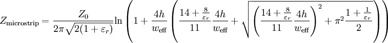
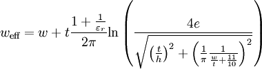
Characteristic ImpedanceA closed-form approximate expression for the quasi-static characteristic impedance of a microstrip line was developed by Wheeler:[4][5][6] where weff is the effective width, which is the actual width of the strip, plus a correction to account for the non-zero thickness of the metallization. The effective width is given by with
This formula is asymptotic to an exact solution in three different cases
It is claimed that for most other cases, the error in impedance is less than 1%, and is always less than 2%.[6] By covering all aspect-ratios in one formula, Wheeler 1977 improves on Wheeler 1965[5] which gives one formula for w / h > 3.3 and another for Curiously, Harold Wheeler disliked both the terms 'microstrip' and 'characteristic impedance', and avoided using them in his papers. BendsIn order to build a complete circuit in microstrip, it is often necessary for the path of a strip to turn through a large angle. An abrupt 90° bend in a microstrip will cause a significant portion of the signal on the strip to be reflected back towards its source, with only part of the signal transmitted on around the bend. One means of effecting a low-reflection bend, is to curve the path of the strip in an arc of radius at least 3 times the strip-width.[7] However, a far more common technique, and one which consumes a smaller area of substrate, is to use a mitred bend. To a first approximation, an abrupt un-mitred bend behaves as shunt capacitance placed between the ground plane and the bend in the strip. Mitring the bend reduces the area of metallization, and so removes the excess capacitance. The percentage mitre is the cut-away fraction of the diagonal between the inner and outer corners of the un-mitred bend. The optimum mitre for a wide range of microstrip geometries has been determined experimentally by Douville and James.[8] They find that a good fit for the optimum percentage mitre is given by, subject to For both the curved and mitred bends, the electrical length is somewhat shorter than the physical path-length of the strip. References
See also
|
|
| This article is licensed under the GNU Free Documentation License. It uses material from the Wikipedia article "Microstrip". A list of authors is available in Wikipedia. |


 dielectric constant of substrate,
 , any
, any  (parallel plate transmission line),
 ,
,  (wire above a ground-plane) and

 (thus introducing a discontinuity in the result at
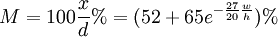
 and the with the substrate dielectric constant
  . This formula is entirely independent of
 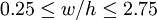 and
and  . They report a VSWR of better than 1.1 (i.e. a return better than -26dB) for any percentage mitre within 4% (of the original
 Last viewed


