To use all functions of this page, please activate cookies in your browser.
My watch list
my.chemeurope.com
my.chemeurope.com
With an accout for my.chemeurope.com you can always see everything at a glance – and you can configure your own website and individual newsletter.
- My watch list
- My saved searches
- My saved topics
- My newsletter
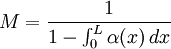
Avalanche photodiodeAvalanche photodiodes (APDs) are photodetectors that can be regarded as the semiconductor analog to photomultipliers. By applying a high reverse bias voltage (typically 100-200 V in silicon), APDs show an internal current gain effect (around 100) due to impact ionization (avalanche effect). However, some silicon APDs employ alternative doping and beveling techniques compared to traditional APDs that allow greater voltage to be applied (> 1500 V) before breakdown is reached and hence a greater operating gain (> 1000). In general, the higher the reverse voltage the higher the gain. Among the various expressions for the APD multiplication factor (M), an instructive expression is given by the formula where L is the space charge boundary for electrons and α is the multiplication coefficient for electrons (and holes). This coefficient has a strong dependence on the applied electric field strength, temperature, and doping profile. Since APD gain varies strongly with the applied reverse bias and temperature, it is necessary to control the reverse voltage in order to keep a stable gain. Avalanche photodiodes therefore are more sensitive compared to other semiconductor photodiodes. If very high gain is needed (105 to 106), certain APDs can be operated with a reverse voltage above the APD's breakdown voltage. In this case, the APD needs to have its signal current limited and quickly diminished. Active and passive current quenching techniques have been used for this purpose. APDs that operate in this high-gain regime are in Geiger mode. This mode is particularly useful for single photon detection provided that the dark count event rate is sufficiently low. A typical application for APDs is laser range finders and long range fiber optic telecommunication. New applications include positron emission tomography and particle physics [1]. APD arrays are becoming commercially available. APD applicability and usefulness depends on many parameters. Some of the larger factors are: quantum efficiency which is an indication of how well incident optical photons are absorbed and then used to generate primary charge carriers, total leakage current which is the sum of the dark current and photocurrent and noise. Electronic dark noise components are series and parallel noise. Series noise, which is the effect of shot noise, is basically proportional to the APD capacitance while the parallel noise is associated with the fluctuations of the APD bulk and surface dark currents. Another noise source is the excess noise factor (F). It describes the statisitical noise that is inherent with the stochastic APD multiplication process. Product highlight
MaterialsIn principle any semiconductor material can be used as a multiplication region:
Excess noiseAs mentioned above, this is the noise due to the multiplication process at a gain, M, and is denoted by F(M) and can often be expressed as: where See alsoReferences
Commercial
|
|
| This article is licensed under the GNU Free Documentation License. It uses material from the Wikipedia article "Avalanche_photodiode". A list of authors is available in Wikipedia. |


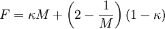
 is the ratio of the hole impact ionization rate to that of electrons. For an electron multiplication device it is given by the hole impact ionization rate divided by the electron impact ionization rate. It is desirable to have a large asymmetry between these rates, in order to minimize

