To use all functions of this page, please activate cookies in your browser.
My watch list
my.chemeurope.com
my.chemeurope.com
With an accout for my.chemeurope.com you can always see everything at a glance – and you can configure your own website and individual newsletter.
- My watch list
- My saved searches
- My saved topics
- My newsletter
ElectromigrationElectromigration is the transport of material caused by the gradual movement of the ions in a conductor due to the momentum transfer between conducting electrons and diffusing metal atoms. The effect is important in applications where high direct current densities are used, such as in microelectronics and related structures. As the structure size in electronics such as integrated circuits (ICs) decreases, the practical significance of this effect increases.
Product highlight
HistoryThe phenomenon of electromigration has been known for over 100 years, having been discovered by the French scientist Gerardin[1]. The topic first became of practical interest in 1966 when the first integrated circuits became commercially available. Research in this field was pioneered by James R. Black, who set the basis for all research in this area and after whom Black's equation is named. At the time the metal interconnects in ICs were still about 10 micrometres wide. Currently interconnects are only hundreds or tens of nanometers in width making research in electromigration increasingly important. Practical implications of electromigrationElectromigration decreases the reliability of ICs. In the worst case it leads to the eventual loss of one or more connections and intermittent failure of the entire circuit. Since the reliability of interconnects is not only of great interest in the field of space travel and for military purposes but also with civilian applications like for example the anti-lock braking system of cars, high technological and economic values are attached to this effect. Due to the relatively high life span of interconnects and the short product lifecycle of most consumer ICs, it is not practical to characterize a product's electromigration under real operating conditions. A mathematical equation, the Black's equation, is commonly used to predict the life span of interconnects in integrated circuits tested under "stress", that is external heating and increased current density, and the model's results can be extrapolated to the device's expected life span under real conditions. Such testing is known as High temperature operating life (HTOL) testing. Although electromigration damage ultimately results in failure of the affected IC, the first symptoms are intermittent glitches, and are quite challenging to diagnose. As some interconnects fail before others, the circuit exhibits seemingly random errors, which may be indistinguishable from other failure mechanisms (such as ESD damage.) In a laboratory setting, electromigration failure is readily imaged with an electron microscope, as interconnect erosion leaves telltale visual markers on the metal layers of the IC. With increasing miniaturization the probability of failure due to electromigration increases in VLSI and ULSI circuits because both the power density and the current density increase. In advanced semiconductor manufacturing processes, copper has replaced aluminium as the interconnect material of choice. Despite its greater fragility in the fabrication process, copper is preferred for its superior conductivity. It is also intrinsically less susceptible to electromigration. However, electromigration continues to be an everpresent challenge to device fabrication, and therefore the EM research for copper interconnects is ongoing (though a relatively new field.) A reduction of the structure (scaling) by a factor k increases the power density proportional to k and the current density increases by k2 whereby EM is clearly strengthened. In modern consumer electronic devices, ICs rarely fail due to electromigration effects. This is because proper semiconductor design practices incorporate the effects of electromigration into the IC's layout. Nearly all IC design houses use automated EDA tools to check and correct electromigration problems at the transistor layout-level. When operated within the manufacturer's specified temperature and voltage range, a properly designed IC-device is more likely to fail from other (environmental) causes, such as cumulative damage from gamma-ray bombardment. Nevertheless, there have been documented cases of product failures due to electromigration. In the late 1980s, one line of Western Digital's desktop drives suffered widespread, predictable failure 12–18 months after field usage. Using forensic analysis of the returned bad units, engineers identified improper design-rules in a third-party supplier's IC controller. By replacing the bad component with that of a different supplier, WD was able to correct the flaw, but not before significant damage to the company's reputation. Overclocking of processors, especially when using higher than nominal voltage, causes electromigration between their transistors and significantly shortens the chips' lifetime. Electromigration can be a cause of degradation in some power semiconductor devices such as low voltage power MOSFETs, in which the lateral current flow through the source contact metallisation (often aluminium) can reach the critical current densities during overload conditions. The degradation of the aluminium layer causes an increase in on-state resistance, and can eventually lead to complete failure. FundamentalsThe material properties of the metal interconnects have a strong influence on the life span. The characteristics are predominantly the composition of the metal alloy and the dimensions of the conductor. The shape of the conductor, the crystallographic orientation of the grains in the metal, procedures for the layer deposition, heat treatment or annealing, characteristics of the passivation and the interface to other materials also affect the durability of the interconnects. There are also grave differences with time dependent current: direct current or different alternating current forms cause different effects. Forces on ions in an electrical fieldTwo forces affect ionized atoms in a conductor. The direct electrostatic force Fe as a result from the electric field therefore having the same direction. The force from the exchange of momentum with other charge carriers Fp showing toward the flow of charge carriers. In metallic conductors Fp is caused by a so-called "electron wind" or "Ion wind". The resulting force Fres on an activated ion in the electrical field is 
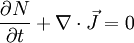
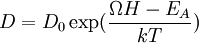
Failure mechanismsDiffusion mechanismsIn a homogeneous crystalline structure, because of the uniform lattice structure of the metal ions, there is hardly any momentum transfer between the conduction electrons and the metal ions. However, this symmetry does not exist at the grain boundaries and material interfaces, and so here momentum is transferred much more vigorously. Since the metal ions in these regions are bonded more weakly than in a regular crystal lattice, once the electron wind has reached a certain strength, atoms become separated from the grain boundaries and are transported in the direction of the current. This direction is also influenced by the grain boundary itself, because atoms tend to move along grain boundaries. Diffusion processes caused by electromigration can be divided into grain boundary diffusion, bulk diffusion and surface diffusion. In general, grain boundary diffusion is the major electromigration process in aluminum wires, whereas surface diffusion is dominant in copper interconnects. Thermal effectsIn an ideal conductor, where atoms are arranged in a perfect lattice structure, the electrons moving through it would experience no collisions and electromigration would not occur. In real conductors, defects in the lattice structure and the random thermal vibration of the atoms about their positions causes electrons to collide with the atoms and scatter, which is the source of electrical resistance (at least in metals; see electrical conduction). Normally, the amount of momentum imparted by the relatively low-mass electrons is not enough to permanently displace the atoms. However, in high-power situations (such as with the increasing current draw and decreasing wire sizes in modern VLSI microprocessors), if many electrons bombard the atoms with enough force to become significant, this will accelerate the process of electromigration by causing the atoms of the conductor to vibrate further from their ideal lattice positions, increasing the amount of electron scattering. High current density increases the number of electrons scattering against the atoms of the conductor, and hence the speed at which those atoms are displaced. In integrated circuits, electromigration does not occur in semiconductors directly, but in the metal interconnects deposited onto them (see semiconductor device fabrication). Electromigration is exacerbated by high current densities and the Joule heating of the conductor (see electrical resistance), and can lead to eventual failure of electrical components. Localized increase of current density is known as current crowding. Balance of atom concentrationA governing equation which describes the atom concentration evolution throughout some interconnect segment, is the conventional mass balance (continuity) equation
where Assuming a vacancy mechanism for atom diffusion we can express D as a function of the hydrostatic stress Electromigration-aware designElectromigration reliability of a wire (Black's equation)At the end of the 1960s J. R. Black developed an empirical model to estimate the MTTF (mean time to failure) of a wire , taking electromigration into consideration:
Here A is a constant based on the cross-sectional area of the interconnect, J is the current density, Ea is the activation energy (e.g. 0.7 eV for grain boundary diffusion in aluminum), k is the Boltzmann constant, T is the temperature and n a scaling factor (usually set to 2 according to Black). It is clear that current density J and (less so) the temperature T are deciding factors in the design process that affect electromigration. The temperature of the conductor appears in the exponent, i.e. it strongly affects the MTTF of the interconnect. For an interconnect to remain reliable in rising temperatures, the maximum tolerable current density of the conductor must necessarily decrease. Wire materialIt is known that pure copper used for Cu-metallization is more electromigration-robust than aluminum. Copper wires can withstand approximately five times more current density than aluminum wires while assuming similar reliability requirements. This is mainly due to the higher electromigration activation energy levels of copper caused by its superior electrical and thermal conductivity as well as its higher melting point. Bamboo structure and metal slottingIt is obvious that a wider wire results in smaller current density and, hence, less likelihood of electromigration. However, if you reduce wire width to below the average grain size of the wire material, the resistance to electromigration increases, despite an increase in current density. This apparent contradiction is caused by the position of the grain boundaries, which in such narrow wires as in a bamboo structure lie perpendicular to the width of the whole wire. Because the grain boundaries in these so-called “bamboo structures” are at right angles to the current flow, the boundary diffusion factor is excluded, and material transport is correspondingly reduced. However, the maximum wire width possible for a bamboo structure is usually too narrow for signal lines of large-magnitude currents in analog circuits or for power supply lines. In these circumstances, slotted wires are often used, whereby rectangular holes are carved in the wires. Here, the widths of the individual metal structures in between the slots lie within the area of a bamboo structure, while the resulting total width of all the metal structures meets power requirements. Blech lengthThere is a lower limit for the length of the interconnect that will allow electromigration to occur. It is known as “Blech length”, and any wire that has a length below this limit will not fail by electromigration. Here, a mechanical stress buildup causes a reversed migration process which reduces or even compensates the effective material flow towards the anode. The Blech length must be considered when designing test structures for electromigration. Via arrangements and corner bendsParticular attention must be paid to vias and contact holes, because generally the ampacity of a (tungsten) via is less than that of a metal wire of the same width. Hence multiple vias are often used, whereby the geometry of the via array is very significant: Multiple vias must be organized such that the resulting current flow is distributed as evenly as possible through all the vias.
Electromigration in Solder JointsThe typical current density at which electromigration occurs in Cu or Al interconnects is 106 to 107 A/cm2. For solder joints (SnPb or SnAgCu lead-free) used in IC chips, however, electromigration occurs at much lower current densities, e.g. 104 A/cm2. It causes a net atom transport along the direction of electron flow. The atoms pile up at the anode, voids are generated at the cathode and back stress is induced during electromigration. The typical failure of a solder joint due to electromigration will occur at the cathode side. Due to the current crowding effect, voids form first at the corner of the solder joint. Then the voids extend and cause a failed circuit. See also
Literature
Reference standards
|
|
| This article is licensed under the GNU Free Documentation License. It uses material from the Wikipedia article "Electromigration". A list of authors is available in Wikipedia. |


 is the atom concentration at the point with a coordinates
  at the moment of time
 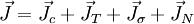 . Define the fluxes mentioned above.
 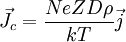 . Here
  is the local current density,
  is the time and position dependent atom diffusivity.
 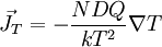 . We use
 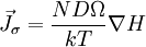 here
here 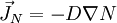 .
.
 where
where 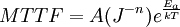
Last viewed


