Pulling crystals for semiconductor technology
Parallel production reduces energy consumption by two thirds
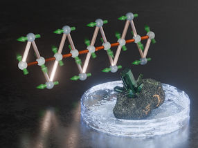
Crystalline semiconductor components form the core of many modern communication technologies such as computers and mobile phones. They are produced during a multi-day pulling process that uses considerable energy. The BINE-Projektinfo brochure “Efficient production of monocrystalline semiconductors” (01/2015) presents a new method for producing gallium arsenide Crystals. Instead of growing individual crystals as was previously the case, nine crystals are now grown in parallel from the melt. This reduces the specific energy consumption for the production by two thirds.
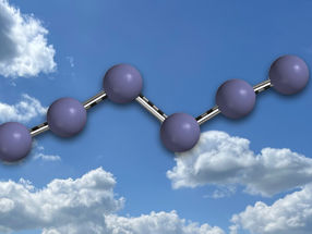
In addition to silicon, which still dominates semiconductor technology, gallium arsenide has also established itself as a substrate material for high-purity single crystals. With these crystals the atoms are arranged in an almost perfect lattice, whereby only every millionth atom is a foreign element. The crystals are pulled from hot melt, which has a temperature of up to 1,300 °C, during a process that takes several days. With the new method, the developers have succeeded in increasing both the solidification rate and yield. The challenge with parallel growth is to supply the heat and arrange the nine crystals in such a manner that the structure and purity of the final product are not impaired.
The new method has been developed by the Freiberger Compound Materials (FCM) company. Dr Berndt Weinert, R&D Manager at FCM: “The method has proved itself in practice and the production has almost completely moved over to using it. An estimated 4,000 MWh were saved in 2014.” The company has since then converted its entire production to the new method.

Other news from the department science