Pushing the resolution limits of scattering near-field optical microscopy
A valuable tool for characterizing surfaces with atomic-scale precision
Advertisement


Researchers have developed a new microscope that can visualize the optical response of surfaces at an unprecedented spatial resolution of one nanometer. This paves the way for optical microscopy of atomic-scale structures, such as single molecules and atomic defects. Such capability is important for optical engineering of nanomaterials and surfaces at angstrom scales.

Fritz-Haber-Institut
Understanding the interaction between light and matter at the smallest scales (angstrom scale) is essential for advancing technology and materials science. Atomic-scale structures, such as defects in diamonds or molecules in electronic devices, can significantly influence a material's optical properties and functionality. To explore these tiny structures, we need to extend the capabilities of optical microscopy.
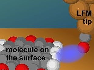
Researchers at the Department of Physical Chemistry at the Fritz-Haber Institute have developed an approach to scattering-type scanning near-field optical microscopy (s-SNOM) that achieves a spatial resolution of 1 nanometer. This technique, termed as ultralow tip oscillation amplitude s-SNOM (ULA-SNOM), combines advanced microscopy methods to visualize materials at the atomic level.
Traditional s-SNOM methods, which use a laser-illuminated probe tip to scan surfaces, typically achieve resolutions of 10 to 100 nanometers. However, this is insufficient for atomic-scale imaging. By integrating s-SNOM with noncontact atomic force microscopy (nc-AFM) and using a silver tip under visible laser illumination, the researchers created a plasmonic cavity (a specialized light field), confined to a tiny volume. This allows for detailed optical contrast at the angstrom scale.
This approach enables scientists to study materials at the smallest scales, potentially leading to advancements in designing new materials for electronics or medical devices. The ability to image features like atomic defects and nanoscale structures with such precision opens new possibilities for optical engineering and materials science.
In summary, this development provides a valuable tool for characterizing surfaces with atomic-scale precision, contributing to future advancements in single-molecule and atomic-scale optical microscopy.


Other news from the department science


