To use all functions of this page, please activate cookies in your browser.
My watch list
my.chemeurope.com
my.chemeurope.com
With an accout for my.chemeurope.com you can always see everything at a glance – and you can configure your own website and individual newsletter.
- My watch list
- My saved searches
- My saved topics
- My newsletter
Chemical vapor deposition
Chemical vapor deposition (CVD) is a chemical process used to produce high-purity, high-performance solid materials. The process is often used in the semiconductor industry to produce thin films. In a typical CVD process, the wafer (substrate) is exposed to one or more volatile precursors, which react and/or decompose on the substrate surface to produce the desired deposit. Frequently, volatile byproducts are also produced, which are removed by gas flow through the reaction chamber. Microfabrication processes widely use CVD to deposit materials in various forms, including: monocrystalline, polycrystalline, amorphous, and epitaxial. These materials include: silicon, carbon fiber, carbon nanofibers, filaments, carbon nanotubes, SiO2, silicon-germanium, tungsten, silicon carbide, silicon nitride, silicon oxynitride, titanium nitride, and various high-k dielectrics. The CVD process is also used to produce synthetic diamonds. Product highlight
Types of chemical vapor depositionA number of forms of CVD are in wide use and are frequently referenced in the literature. These processes differ in the means by which chemical reactions are initiated (e.g., activation process) and process conditions.
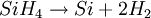
Substances commonly deposited for ICsThis section discusses the CVD processes often used for integrated circuits (ICs). Particular materials are deposited best under particular conditions. PolysiliconPolycrystalline silicon is deposited from silane (SiH4), using the following reaction: This reaction is usually performed in LPCVD systems, with either pure silane feedstock, or a solution of silane with 70-80% nitrogen. Temperatures between 600 and 650 °C and pressures between 25 and 150 Pa yield a growth rate between 10 and 20 nm per minute. An alternative process uses a hydrogen-based solution. The hydrogen reduces the growth rate, but the temperature is raised to 850 or even 1050 °C to compensate. Polysilicon may be grown directly with doping, if gases such as phosphine, arsine or diborane are added to the CVD chamber. Diborane increases the growth rate, but arsine and phosphine decrease it. Silicon dioxideSilicon dioxide (usually called simply "oxide" in the semiconductor industry) may be deposited by several different processes. Common source gases include silane and oxygen, dichlorosilane (SiCl2H2) and nitrous oxide (N2O), or tetraethylorthosilicate (TEOS; Si(OC2H5)4). The reactions are as follows:
The choice of source gas depends on the thermal stability of the substrate; for instance, aluminium is sensitive to high temperature. Silane deposits between 300 and 500 °C, dichlorosilane at around 900 °C, and TEOS between 650 and 750 °C. However, silane produces a lower-quality oxide than the other methods (lower dielectric strength, for instance), and it deposits nonconformally. Any of these reactions may be used in LPCVD, but the silane reaction is also done in APCVD. CVD oxide invariably has lower quality than thermal oxide, but thermal oxidation can only be used in the earliest stages of IC manufacturing. Oxide may also be grown with impurities (alloying or "doping"). This may have two purposes. During further process steps that occur at high temperature, the impurities may diffuse from the oxide into adjacent layers (most notably silicon) and dope them. Oxides containing 5% to 15% impurities by mass are often used for this purpose. In addition, silicon dioxide alloyed with phosphorus pentoxide ("P-glass") can be used to smooth out uneven surfaces. P-glass softens and reflows at temperatures above 1000 °C. This process requires a phosphorus concentration of at least 6%, but concentrations above 8% can corrode aluminium. Phosphorus is deposited from phosphine gas and oxygen:
Glasses containing both boron and phosphorus (borophosphosilicate glass, BPSG) undergo viscous flow at lower temperatures; around 850 °C is achievable with glasses containing around 5 weight % of both constituents, but stability in air can be difficult to achieve. Phosphorus oxide in high concentrations interacts with ambient moisture to produce phosphoric acid. Crystals of BPO4 can also precipitate from the flowing glass on cooling; these crystals are not readily etched in the standard reactive plasmas used to pattern oxides, and will result in circuit defects in integrated circuit manufacturing. Besides these intentional impurities, CVD oxide may contain byproducts of the deposition process. TEOS produces a relatively pure oxide, whereas silane introduces hydrogen impurities, and dichlorosilane introduces chlorine. Lower temperature deposition of silicon dioxide and doped glasses from TEOS using ozone rather than oxygen has also been explored (350 to 500 °C). Ozone glasses have excellent conformality but tend to be hygroscopic -- that is, they absorb water from the air due to the incorporation of silanol (Si-OH) in the glass. Infrared spectroscopy and mechanical strain as a function of temperature are valuable diagnostic tools for diagnosing such problems. Silicon nitrideSilicon nitride is often used as an insulator and chemical barrier in manufacturing ICs. The following two reactions deposit nitride from the gas phase:
Silicon nitride deposited by LPCVD contains up to 8% hydrogen. It also experiences strong tensile stress (physics), which may crack films thicker than 200 nm. However, it has higher resistivity and dielectric strength than most insulators commonly available in microfabrication (1016 Ω·cm and 10 MV/cm, respectively). Another two reactions may be used in plasma to deposit SiNH:
These films have much less tensile stress, but worse electrical properties (resistivity 106 to 1015 Ω·cm, and dielectric strength 1 to 5 MV/cm). MetalsSome metals (notably aluminium and copper) are seldom or never deposited by CVD. As of 2002, a viable CVD process for copper did not exist, and the metal was deposited by electroplating. Aluminium can be deposited from tri-isobutyl aluminium, but physical vapor deposition methods are usually preferred. However, CVD processes for molybdenum, tantalum, titanium and tungsten are widely used. These metals can form useful silicides when deposited onto silicon. Mo, Ta and Ti are deposited by LPCVD, from their pentachlorides. In general, for an arbitrary metal M, the reaction is as follows:
The usual source for tungsten is tungsten hexafluoride, which may be deposited in two ways:
See also
References
|
|
| This article is licensed under the GNU Free Documentation License. It uses material from the Wikipedia article "Chemical_vapor_deposition". A list of authors is available in Wikipedia. |

Last viewed


