NIST Unveils Atom-based Standards For Measuring Chip Features Under 50 Nanometers
Device features on computer chips as small as 40 nanometers (nm) wide-less than one-thousandth the width of a human hair-can now be measured reliably thanks to new test structures developed by a team of physicists, engineers, and statisticians at the Commerce Department's National Institute of Standards and Technology (NIST), SEMATECH, and other collaborators. The test structures are replicated on reference materials that will allow better calibration of tools that monitor the manufacturing of microprocessors and similar integrated circuits.
The new test structures are the culmination of NIST's more than four-year effort to provide standard "rulers" for measuring the narrowest linear features that can be controllably etched into a chip. The NIST rulers are precisely etched lines of crystalline silicon ranging in width from 40 nm to 275 nm. The spacing of atoms within the box-shaped silicon crystals is used like hash marks on a ruler to measure the dimensions of these test structures. Industry can use these reference materials to calibrate tools to reliably measure microprocessor-device gates, for example, which control the flow of electrical charges in chips.
The new reference materials, configured as a 9 millimeter (mm) by 11 mm chip embedded in a silicon wafer, are now being evaluated by SEMATECH member companies. Compared to a batch of prototype test structures produced by NIST in 2001, the new reference materials offer a wider range of reference feature sizes, including some that are much narrower, and they are measured much more precisely (with uncertainties of less than 2 nm compared to 14 nm previously). In the absence of reference materials such as these, companies have calibrated measurement tools using in-house standards, which may neither be accurate nor agree with each other.
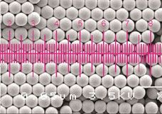
The new silicon reference materials are the outcome of a series of technical and procedural innovations. First, rows of rectangular features are etched into a particular type of silicon wafer in which atoms are arranged in a regular lattice design. The features are about 150 nm high, arrayed in sets of six features, each with a different width. The lattice has extremely even edges, but NIST modified the etching process to make the sides of the features even smoother, which helped to improve measurement precision. Illustration of silicon crystals showing how the interlocked cubic structure produces planes of atoms that can be used like hash marks on a ruler
Using four different types of microscopes-optical, scanning electron (SEM), atomic force (AFM), and high-resolution scanning transmission microscopes (HRTEM)-the silicon reference features are first screened to identify those with the approximate right dimensions, and then very carefully measured. A key step in the calibration process involves passing a beam of electrons through the silicon lines to a detector. Alternating dark and light parallel lines on the detector mark where columns of silicon atoms diffract the electrons. Technicians then manually counted these marks. From this count, the dimension of the reference feature can be calculated, because the number of lines in the image matches the number of silicon atoms in the crystal, whose spacing is always exactly the same and is traceable to the international standard of length. These data can then be used to calibrate measurements by other microscope tools.
Other news from the department research and development


These products might interest you
Starna by Starna Scientific
Highest quality precision quartz and glass cuvettes for all applications
Custom and OEM options. All popular cells available from stock!
Certified Reference Materials for Spectroscopy by Starna Scientific
Starna Scientific: Your solution for precise spectroscopy calibration
ISO-certified reference materials for accurate and safe spectroscopy
Certified reference materials of the European Commission's Joint Research Centre by ERM
Certified reference materials for the analysis of environmental,food,clinical and industrial samples
Certified reference materials (CRMs) provide confidence in the correctness of analytical results
SmartCal by Mettler-Toledo
SmartCal verifies Moisture Analyzer Performance in 10 minutes
Proper verification and documentation assists you to fulfill the demands of industry regulations and company audits
NanoStandard™ / MicroStandard™ by Applied Microspheres
Highly uniform polymer particle size standards, with traceable mean diameters
Traceable both to the international System of Units (SI) and NIST