New polymer could improve semiconductor manufacturing, packaging
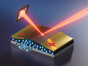
Researchers at Rensselaer Polytechnic Institute and Polyset Company have developed a new inexpensive, quick-drying polymer that could lead to dramatic cost savings and efficiency gains in semiconductor manufacturing and computer chip packaging. Along with allowing enhanced performance and cost savings for conventional photolithography processes, the new material, called polyset epoxy siloxane (PES), should also enable a new generation of lower-cost, on-chip nanoimprinting lithography technology, according to the researchers.
"With this new material, chip manufacturers will be able to trim several steps from their production and packaging processes, and in turn realize a cost savings," said Toh-Ming Lu, the R.P. Baker Distinguished Professor of Physics at Rensselaer, who oversaw the study. "PES is cheaper and more reliable."
The widely adopted technique of photolithography involves using a mix of light and chemicals to generate intricate micro- and nano-scale patterns on tiny areas of silicon. As part of the process, a thin polymer film - called a redistribution layer, and crucial to the effectiveness of device - is deposited onto the silicon wafer, in order to ease the signal propagation delay and to protect the chip from different environmental and mechanical factors.
The new PES material developed by Lu's group and Polyset Company is one such thin polymer film, and it offers several advantages over the incumbent materials typically used in the semiconductor manufacturing industry. In addition, their new PES material can also be used as a thin polymer film for ultraviolet (UV) on-chip nanoimprinting lithography technology, which is still in the early phases of development. The consistency of using PES in conventional technology, and then continuing to use PES while academia and industry test and gradually migrate to the next generation of devices, should help ease the transition, Lu said.
Original publication: Journal of Vacuum Science and Technology B.
Other news from the department science


Get the chemical industry in your inbox
From now on, don't miss a thing: Our newsletter for the chemical industry, analytics, lab technology and process engineering brings you up to date every Tuesday and Thursday. The latest industry news, product highlights and innovations - compact and easy to understand in your inbox. Researched by us so you don't have to.