To use all functions of this page, please activate cookies in your browser.
My watch list
my.chemeurope.com
my.chemeurope.com
With an accout for my.chemeurope.com you can always see everything at a glance – and you can configure your own website and individual newsletter.
- My watch list
- My saved searches
- My saved topics
- My newsletter
Fermi surfaceIn condensed matter physics, the Fermi surface is an abstract boundary useful for predicting the thermal, electrical, magnetic, and optical properties of metals, semimetals, and doped semiconductors. The shape of the Fermi surface is derived from the periodicity and symmetry of the crystalline lattice and from the occupation of electronic energy bands. The existence of a Fermi surface is a direct consequence of the Pauli exclusion principle, which prevents fermions from all crowding into the same state. Additional recommended knowledge
TheoryFormally speaking, the Fermi surface is a surface of constant energy in
Materials with complex crystal structures can have quite intricate Fermi surfaces. The figure illustrates the anisotropic Fermi surface of graphite, which has both electron and hole pockets in its Fermi surface due to multiple bands crossing the Fermi energy along the The state occupancy of fermions like electrons is governed by Fermi-Dirac statistics so at finite temperatures the Fermi surface is accordingly broadened. In principle all fermion energy level populations are bound by a Fermi surface although the term is not generally used outside of condensed-matter physics. Experimental determinationde Haas-van Alphen effect. Electronic Fermi surfaces have been measured through observation of the oscillation of transport properties in magnetic fields H, for example the de Haas-van Alphen effect (dHvA) and the Shubnikov-De Haas effect (SdH). The former is an oscillation in magnetic susceptibility and the latter in resistivity. The oscillations are periodic versus 1 / H and occur because of the quantization of energy levels in the plane perpendicular to a magnetic field, a phenomenon first predicted by Lev Landau. The new states are called Landau levels and are separated by an energy Observation of the dHvA and SdH oscillations requires magnetic fields large enough that the circumference of the cyclotron orbit is smaller than a mean free path. Therefore dHvA and SdH experiments are usually performed at high-field facilities like the High Field Magnet Laboratory in Netherlands, Grenoble High Magnetic Field Laboratory in France, the Tsukuba Magnet Laboratory in Japan or the National High-Field Magnet Lab in the United States.
Angle resolved photoemission. The most direct experimental technique to resolve the electronic structure of crystals in the momentum-energy space (see reciprocal lattice), and, consequently, the Fermi surface, is the angle resolved photoemission spectroscopy (ARPES). An example of the Fermi surface of superconducting cuprates measured by ARPES is shown in figure. Two photon positron annihilation. With positron annihilation the two photons carry the momentum of the electron away; as the momentum of a thermalized positron is negligible, in this way also information about the momentum distribution can be obtained. Because the positron can be polarized, also the momentum distribution for the two spin states in magnetized materials can be obtained. Another advantage with De Haas-Van Alphen-effect is that the technique can be applied to non-dilute alloys. In this way the first determination of a smeared Fermi surface in a 30% alloy has been obtained in 1978. References
See Also |
|
| This article is licensed under the GNU Free Documentation License. It uses material from the Wikipedia article "Fermi_surface". A list of authors is available in Wikipedia. |


 -space where
 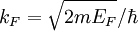 determined by the valence electron concentration where
  is the reduced Planck's constant. A material whose Fermi level falls in a gap between bands is an
  direction. Often in a metal the Fermi surface radius
  where a is the
  where
where  ) perpendicular to the magnetic field direction
  by the equation
 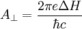 . Thus the determination of the periods of oscillation for various applied field directions allows mapping of the Fermi surface.
Last viewed

