To use all functions of this page, please activate cookies in your browser.
My watch list
my.chemeurope.com
my.chemeurope.com
With an accout for my.chemeurope.com you can always see everything at a glance – and you can configure your own website and individual newsletter.
- My watch list
- My saved searches
- My saved topics
- My newsletter
HeterojunctionA heterojunction is the interface that occurs between two layers or regions of dissimilar crystalline semiconductors. These semiconducting materials have unequal band gaps as opposed to a homojunction. It is often advantageous to engineer the electronic energy bands in many solid state device applications including semiconductor lasers, solar cells and transistors to name a few. The combination of multiple heterojunctions together in a device is called a heterostructure although the two terms are commonly used interchangeably. The requirement that each material be a semiconductor with unequal band gaps is somewhat loose especially on small length scales where electronic properties depend on spatial properties. A more modern definition may be to say that a heterojunction is the interface between any two solid state materials including crystalline and amorphous structures of metallic, insulating, fast ion conductor and semiconducting material. In 2000, the Nobel Prize was awarded with one half jointly to Herbert Kroemer (University of California at Santa Barbara, California, USA) and Zhores I. Alferov (A.F. Ioffe Physico-Technical Institute, St. Petersburg, Russia) for "developing semiconductor heterostructures used in high-speed- and opto-electronics" Product highlight
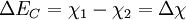
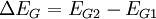
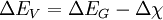
Energy band offsets for ideal heterojunctionsSemiconductor interfaces can be organized into three types of heterojunctions: straddling gap (type I), staggered gap (type II) or broken gap (type III) as seen in the figure above. There are three relevant material properties for classifying a given junction and understanding the charge dynamics at a heterojunction: band gap, electron affinity and work function. The energy difference between the valence band (VB) and conduction band (CB), called the band gap, is anywhere from 0eV for a metal (there is no gap) to over 4eV for an insulator. The work function of a material is the energy difference between the fermi energy (chemical equilibrium energy) and the vacuum level (where electron removal occurs). Finally the electron affinity of each material is needed which is the energy difference between the conduction band and the vacuum level. Calculating energy band offsets for an ideal heterojunction is straightforward given these material properties using the Anderson's rule. The conduction band offset depends only on the electron affinity difference between the two semiconductors:
Then using the change in band gap:
The valence band offset is simply given by:
Which confirms the trivial relationship between band offsets and band gap difference:
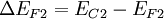
In Anderson's idealized model these material parameters are unchanged when the materials are brought together to form an interface, so it ignores the quantum size effect, defect states and other perturbations which may or may not be the result of imperfect crystal lattice matches (more on lattice considerations below). When two materials are brought together and allowed to reach chemical/thermal equilibrium the fermi level in each material aligns and is constant throughout the system. To the extent that they are able, electrons in the materials leave some regions (depletion) and build up in others (accumulation) in order to find equilibrium. When this occurs a certain amount of band bending occurs near the interface. This total band bending can be quantified with the built in potential given by:
Where In most cases where the materials are undoped, these ΔEF terms are just half the band gap. Otherwise, ΔEF can be calculated with typical solid state device calculations and depends on dopant concentrations and temperature. The built in potential gives the degree to which band bending occurs but tells us nothing about how this happens spatially. In order to know over what distance the bending occurs in which materials, we must know the density of states and state occupation given by the [Fermi-Dirac distribution]]. Energy band offsets in real heterojunctions
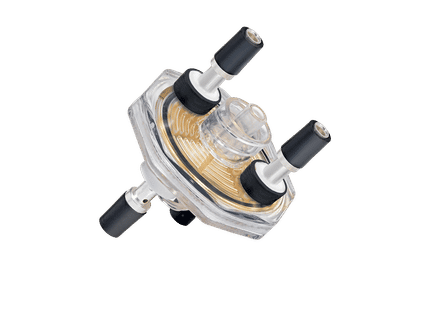
In real semiconductor heterojunctions, Anderson's model fails to predict actual band offsets. Some material parameters are given in the table on the right which do not match experimental results using Anderson's rule. This idealized model ignores the fact that each material is made up of a crystal lattice whose electrical properties depend on a periodic arraignment of atoms. This periodicity is broken at the heterojunction interface to varying degrees. In cases where both materials have the same lattice, they may still have differing lattice constants which give rise to crystal strain which changes the band energies. In other cases the strain is relaxed via dislocations and other interfacial defects which also change the band energies. A common anion rule was proposed which guesses that since the valence band is related to anionic states, materials with the same anions should have very small valence band offsets. This however did not explain the data but is related to the trend that two materials with different anions tend to have larger valence band offsets than conduction band offsets. Tersoff2 proposed a model based on more familiar metal-semiconductor junctions where the conduction band offset is given by the difference in Schottky barrier height. This model includes a dipole later at the interface between the two semiconductors which arises from electron tunneling from the conduction band of one material into the gap of the other. This model agrees well with systems where both materials are closely lattice matched1 such as GaAs/AlGaAs. Anderson's rule overestimates the offset in the conduction band of the commercially important type two offset GaAs/AlAs system with ΔEC / ΔEG = .73 from the data above. It has been shown3 that for the actual ratio is closer ΔEC / ΔEG = .6. This is known as the 60:40 rule and applies to heterojunctions of GaAs with all compositions of AlGaAs. The typical method for measuring band offsets is by calculating them from measuring exciton energies in the luminescence spectra3. Nanoscale heterojunctionsIn quantum dots the band energies are dependent on crystal size due to the quantum size effect. This enables band offset engineering in nanoscale heterostructures. It is possible4 to use the same materials but change the type of junction, say from straddling (type I) to staggered (type II), by changing the size or thickness of the crystals involved. The most common nanoscale heterostructure system is core\shell CdSe\ZnS which is a straddling gap (type I) offset. In this system the much larger band gap ZnS passivates the surface of the fluorescent CdSe core thereby increasing the quantum efficiency of the luminescence. There is an added bonus of increased thermal stability due to the stronger bonds in the ZnS shell as suggested by its larger band gap. Since CdSe and ZnS both grow in the zincblende crystal phase and are closely lattice matched, core shell growth is preferred. In other systems or under different growth conditions it may be possible to grow anisotropic structures such as the one seen in the image on the right It has been shown5 that the driving force for charge transfer between conduction bands in these structures is the conduction band offset. By decreasing the size of CdSe nanocrystals grown on TiO2 Robel et. al5 found that electrons transfered faster from the higher CdSe conduction band into TiO2. In CdSe the quantum size effect is much more pronounced in the conduction band due to the smaller effective mass than in the valence band and this is the case with most semiconductors. Consequently, engineering the conduction band offset is typically much easier with nanoscale heterojunctions. For staggered (type II) offset nanoscale heterojunctions, photo-induced charge separation can occur since there the lowest energy state for holes may be on one side of the junction where as the lowest energy for electrons is on the opposite side. It has been suggested5 that anisotropic staggered gap (type II) nanoscale heterojunctions may be used for photo catalysis, specifically for water splitting with solar energy. ApplicationsUsing heterojunctions in lasers was first proposed6 in 1963 when Herbert Kroemer, thought of as the father of this field, suggested that population inversion could be greatly enhanced by haterostructures. By incorporating a smaller direct band gap material like GaAs between two larger band gap layers like AlAs, carriers can be confined so that lasing can occur at room temperature with low threshold currents. It took many years for the material science of heterostructure fabrication to catch up with Kroemer's ideas but now it is the industry standard. It was later discovered that the bad gap could be controlled by taking advantage of the quantum size effect in quantum well heterostructures. Furthermore, heterostructures can be used as waveguides to the the index step which occurs at the interface, another major advantage to their use in semiconductor lasers. Semiconductor diode lasers used in CD & DVD players and fiber optic transceivers are manufactured using alternating layers of various III-V and II-VI compound semiconductors to form lasing heterostructures. When a heterojunction is used as the base-emitter junction of a bipolar junction transistor, extremely high forward gain and low reverse gain result. This translates into very good high frequency operation (values in tens to hundreds of GHz) and low leakage currents. This device is called a heterojunction bipolar transistor (HBT). Heterojunctions are used in high electron mobility transistors (HEMT) which can operate at significantly higher frequencies (over 500 GHz). The proper doping profile and band alignment gives rise to extremely high electron mobilities by creating a two dimensional electron gas within a dopant free region where very little scattering can occur. FabricationHeterojunction manufacturing generally requires the use of molecular beam epitaxy (MBE) or chemical vapor deposition (CVD) technologies into order to precisely control the deposition thickness and create a planar interface. MBE and CVD tend to be very complex and expensive compared to traditional silicon device fabrication. References[1] Pallab, Bhattacharya (1997), , Prentice Hall, ISBN 0134956567 [2] J. Tersoff, Physical Review, B30, 4874, 1984 [3] N. Debbar et al., Physical Review, B40, 1058, 1989 [4] Sergei A. Ivanov, Andrei Piryatinski, Jagjit Nanda, Sergei Tretiak, Kevin R. Zavadil, William O. Wallace, Don Werder and Victor I. Klimov, J. Am. Chem. Soc., 129, 11708-11719, 2007 [5] Istvan Robel, Masaru Kuno and Prashant V. Kamat, J. Am. Chem. Soc., 129, 4136-4137, 2007 [6] H. Kroemer, Proceedings of the IEEE, Vol. 51, pp. 1782-1783, 1963
See also |
||||||||||||||||||||||||||||
| This article is licensed under the GNU Free Documentation License. It uses material from the Wikipedia article "Heterojunction". A list of authors is available in Wikipedia. |


 and
and