Looking down the tube
How defects make nano-objects better
Advertisement


They are extremely light, yet stronger than steel and more resilient than diamond. They are nearly unbeatable as heat and electricity conductors. In some cases, they even become superconductors with no electric resistance: carbon nanotubes are – at a diameter of a few millionths of a millimeter – truly a tiny wonder, and are awakening great hope in all branches of industry from metrology to optoelectronics. An international research group that includes scientists from LMU has now shown that defects in nanotubes can actually make the material better. Selective doping can change the electrical conductivity and other properties of the nanostructures to suit their intended purpose. This work revolved around the new, highly complex microscopy technology dubbed TENOM. The LMU researchers have also used this technology previously to study various nanotube systems in higher resolution than ever before. One of the things they demonstrated was that a complex of nanotubes and DNA makes an ideal sensor for individual molecules – right down to the nanoscale.
Ludwig - Maximilians - Universität Munich
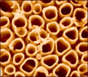
Without carbon, there would be no life on earth. Nanotechnology, too, has to thank this chemical element for an especially promising group of particles: carbon nanotubes. These hollow structures of either a single-walled tubes or multiple, nested tubes were first detected in 1991. They have a diameter of one half to two nanometers, but are many, many times longer. Made up only of carbon hexagons, carbon nanotubes boast a surprising range of properties.
They are lighter than aluminum, stronger than steel and extreme conductors of heat and electricity, achieving even superconductivity. Yet nanotubes have so far largely resisted being used in series production. Once the technical hurdles have been overcome, however, there is a huge number of applications in which they could be used, including electronic components, composite materials and nanomedicine – for transporting drugs through the body, for example.
“The arrangement of the carbon atoms is the key to the properties of nanotubes,” reports Professor Dr. Achim Hartschuh of the Center for NanoScience (CeNS) of LMU Munich. “But their extraordinary optical properties are due to their dimensions: the small diameter at a substantially longer length in comparison makes the structures virtually one-dimensional. It has even been shown that semiconducting nanotubes produce an optical spectrum of their own. We call this photoluminescence.”
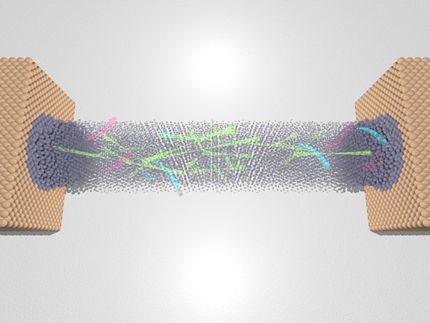
Within the cluster of excellence Nanosystems Initiative Munich (NIM), the physicist and his team have been investigating these nanostructures using "tip-enhanced near-field optical microscopy”, or TENOM for short, which Hartschuh was also prominently involved in developing. TENOM uses a microscopically tiny, extremely sharp gold tip placed within the focus of a laser beam, which probes an object at a distance of just a few nanometers. “This gives us a resolution of about ten nanometers, which exceeds conventional microscopy by a factor of 30,” reports Hartschuh.
This is how he and his research colleagues managed to describe nanotubes with individual defects in their structure in the present study. “We showed that this alters the speed of electrons,” says Hartschuh. “In the vicinity of negatively charged defects, these subatomic particles, which are also negatively charged, become faster, which affects the conductivity of the material. We could then exploit this effect by introducing foreign components into the nanotubes. This doping, as we call it, is already a successful practice in the semiconductor industry.”
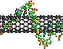
In a previous study under Hartschuh’s leadership, the research group investigated the properties of a complex of nanotubes and DNA. Their relative proportions fit superbly, since our DNA molecule can also form long threads of just a few nanometers in diameter. If nanotubes are dissolved in water, they often form bundles – and these bundles can be dissolved again by DNA. Aside from this purely technical function, however, there is also discussion on using a complex of these two structures as a molecular sensor.
“We took a look at the optical response of nanotubes on being wrapped by individual DNA strands,” says Hartschuh. “As we did this, we also observed the energy transfer between individual nanotubes. It turned out that a complex of nanotubes and DNA could make an ideal sensor, possibly even for detecting individual molecules at a nanoscale. These and all other results are significant for the application of nanotubes in nanoelectronics, nanophotonics, nanosensors, and for our understanding of physical processes at the nanometer scale.”
Original publication: “Electron und phonon renormalization at defect/doping sites in carbon nanotubes”, Indhira O. Maciel et. al., Nature Materials, online 19 October 2008-10-20
“Visualizing the Local Optical Response of Semiconducting Carbon Nanotubes to DNA Wrapping”, Huihong Qian et. al., Nano Letters, Vol. 8, No. 9, p. 2706-2711, 1 August 2008
“Exciton energy Transfer in Pairs of Single-Walled Carbon Nanotubes”, Huihong Qian et. al., Nano Letters, Vol. 8, No. 5, p. 1363-1367, 27 March 2008
Other news from the department science


