A sharper look at the interior of semiconductors
A research team is developing a high-resolution imaging technique that can be used to determine internal structures in materials and their chemical composition in a non-destructive manner and with nanometre precision
Advertisement


Images provide information – what we can observe with our own eyes enables us to understand. Constantly expanding the field of perception into dimensions that are initially hidden from the naked eye, drives science forward. Today, increasingly powerful microscopes let us see into the cells and tissues of living organisms, into the world of microorganisms as well as into inanimate nature. But even the best microscopes have their limits. “To be able to observe structures and processes down to the nanoscale level and below, we need new methods and technologies,” says Dr Silvio Fuchs from the Institute of Optics and Quantum Electronics at the University of Jena. This applies in particular to technological areas such as materials research or data processing. “These days, electronic components, computer chips or circuits are becoming increasingly small,” adds Fuchs. Together with colleagues, he has now developed a method that makes it possible to display and study such tiny, complex structures and even “see inside” them without destroying them. In the current issue of the scientific journal “Optica”, the researchers present their method – coherence tomography with Extreme Ultraviolet Light (XCT for short) – and show its potential in research and application.
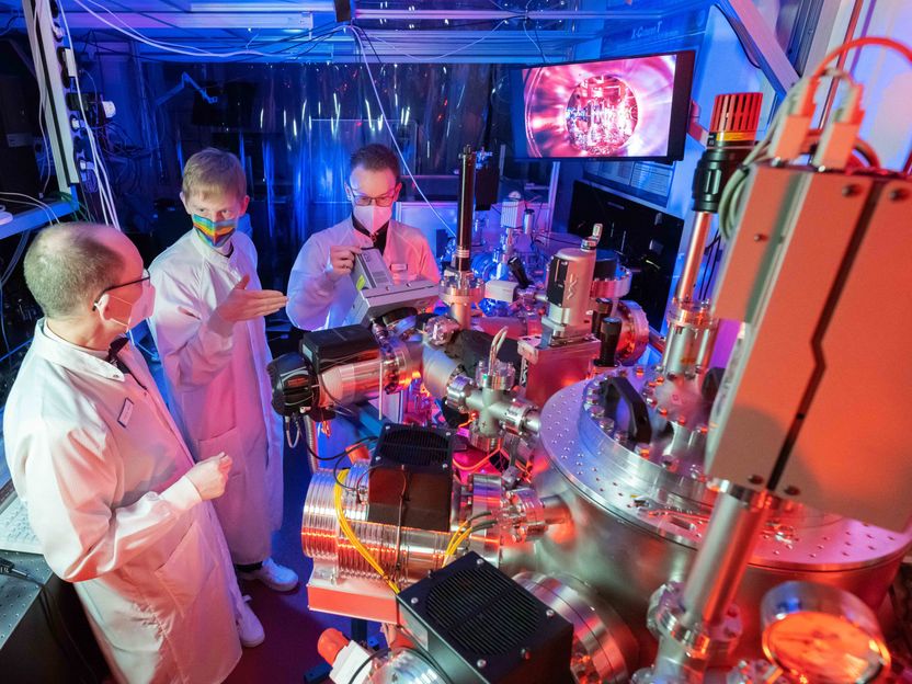
Prof. Dr. Gerhard Paulus, PhD student Felix Wiesner and Dr. Silvio Fuchs (from left) in a laser laboratory.
Jens Meyer (University of Jena)
Light penetrates the sample and is reflected by internal structures
The imaging procedure is based on optical coherence tomography (OCT), which has been established in ophthalmology for a number of years, explains doctoral candidate Felix Wiesner, the lead author of the study. “These devices have been developed to examine the retina of the eye non-invasively, layer by layer, to create 3-dimensional images.” At the ophthalmologist, OCT uses infrared light to illuminate the retina. The radiation is selected in such a way that the tissue to be examined does not absorb it too strongly and it can be reflected by the inner structures. However, the physicists in Jena use extremely short-wave UV light instead of long-wave infrared light for their OCT. “This is due to the size of the structures we want to image,” says Felix Wiesner. In order to look into semiconductor materials with structure sizes of only a few nanometres, light with a wavelength of only a few nanometres is needed.
Nonlinear optical effect generates coherent extremely short-wave UV light
Generating such extremely short-wave UV light (XUV) used to be a challenge and was almost only possible in large-scale research facilities. Jena physicists, however, generate broadband XUV in an ordinary laboratory and use what are called high harmonics for this purpose. This is radiation that is produced by the interaction of laser light with a medium and it has a frequency many times that of the original light.
The higher the harmonic order, the shorter the resulting wavelength.
“In this way, we generate light with a wavelength of between 10 and 80 nanometres using infrared lasers,” explains Prof. Gerhard Paulus, Professor of Nonlinear Optics at the University of Jena. “Like the irradiated laser light, the resulting broadband XUV light is also coherent, which means that it has laser-like properties.”
In the work described in their current paper, the physicists exposed nanoscopic layer structures in silicon to the coherent XUV radiation and analysed the reflected light. The silicon samples contained thin layers of other metals, such as titanium or silver, at different depths. Because these materials have different reflective properties from the silicon, they can be detected in the reflected radiation. The method is so precise that not only can the deep structure of the tiny samples be displayed with nanometre accuracy, but – due to the differing reflective behaviour – the chemical composition of the samples can also be determined precisely and, above all, in a non-destructive manner. “This makes coherence tomography an interesting application for inspecting semiconductors, solar cells or multilayer optical components,” says Paulus. It could be used for quality control in the manufacturing process of such nanomaterials, to detect internal defects or chemical impurities.
Original publication


Other news from the department science


