World's smallest light-emitting diode produced
New ceramic diaphragm enables 2500× higher pixel density
Advertisement


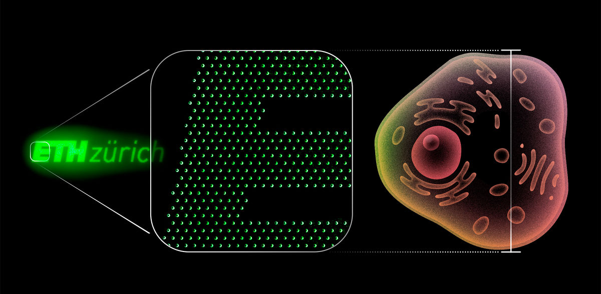
Researchers at ETH Zurich are producing organic light-emitting diodes (OLEDs) on the nanoscale - they are around a hundred times smaller than a human cell. This not only makes ultra-sharp screens and microscopes possible. The pixels are so small that new wave optics applications are conceivable.
miniaturization is the driving force behind the semiconductor industry. The enormous increase in computer performance since the 1950s is largely due to the fact that ever smaller structures can be produced on silicon chips. Chemical engineers at ETH Zurich have now succeeded in reducing the size of organic light emitting diodes (OLEDs), which are mainly used today in premium cell phones and TV screens, by orders of magnitude. Their study was recently published in the specialist journal Nature Photonics.
Miniaturized in one step
Light-emitting diodes are electronic chips made of semiconductor materials that convert electrical current into light. "The diameter of the smallest OLED pixels we have developed to date is in the region of 100 nanometers. This makes them around 50 times smaller than the current state of the art," explains Jiwoo Oh, a doctoral student in ETH Professor Chih-Jen Shih's Nanomaterial Engineering research group.
Oh developed the process for manufacturing the new nano-OLED together with Tommaso Marcato. "The maximum density of the pixels is around 2500 times greater than before in a single step," adds Marcato, who works as a postdoc in Shih's group.
For comparison: until the 2000s, the rate of miniaturization of computer processors followed Moore's Law, according to which the density of electronic elements doubled every two years.
Screens, microscopes and sensors
Pixels in the size range of 100 to 200 nanometers form the basis for ultra-high-resolution screens, which could display razor-sharp images in glasses close to the eye, for example. To illustrate this, the researchers working with Shih have depicted the ETH Zurich logo. This ETH logo consists of 2,800 nano-OLEDs and is similar in size to a human cell. Each of its pixels measures around 200 nanometers (0.2 micrometers). The ETH researchers' smallest pixels to date are in the range of 100 nanometers.
However, the tiny light donors could also help to focus into the sub-micrometer range using high-resolution microscopes. "A nano-pixel field as a light source could illuminate the smallest areas of a sample - the individual images could then be put together in the computer to form an extremely detailed image," explains the professor of technical chemistry. He also sees the potential of nanopixels as tiny sensors that could detect signals from individual nerve cells, for example.
Nano pixels generate optical wave effects
However, the small dimensions also open up possibilities for research and technology that were previously not even feasible, as Marcato emphasizes: "When two light waves of the same colour move closer together than half their wavelength - the so-called diffraction limit - they no longer oscillate independently of each other, but begin to interact with each other." For visible light, this limit is between around 200 and 400 nanometers, depending on the color - and the ETH researchers' nano-OLEDs can also be placed this close together.
The basic principle of interacting waves can be illustrated by throwing two stones next to each other into a mirror-smooth lake. This creates a geometric pattern of wave crests and troughs where the circular water waves meet. In a similar way, cleverly arranged nano-OLEDs can create optical wave effects in which the light from neighboring pixels amplifies or cancels each other out.
Manipulating light direction and polarization
In initial experiments, Shih's team was able to manipulate the direction of the emitted light with the help of such interactions. Instead of emitting light in all directions above the chip, the OLEDs then only emit their light at very specific angles. "In future, it will also be possible to focus the light of a nano-OLED matrix in one direction and thus construct powerful mini lasers," Marcato expects.
Polarized light - i.e. light that only oscillates in one plane - can also be generated using interactions, as the researchers have already shown. This is used today in medicine, for example, to distinguish healthy tissue from cancerous tissue.
Modern radio and radar technologies provide an idea of the potential of interactions. They use wavelengths ranging from millimetres to kilometers and have been using interactions for a long time. So-called phased array arrangements allow antennas or transmitter signals to be specifically aligned and focused.
In the optical spectrum, such technologies could help to further accelerate the transmission of information in data networks and computers.
Ceramic membrane makes the difference
In the manufacture of OLEDs, the light-emitting molecules have so far been subsequently vapor-deposited onto the silicon chips. This is done using relatively thick metal masks, which produce correspondingly larger pixels.
A special ceramic material is now providing the boost in terms of miniaturization, as Oh explains: "Silicon nitride can form very thin yet resilient membranes that do not sag on surfaces in the square millimetre range."
This enabled the researchers to produce templates that are around 3000 times thinner for the placement of the nano-OLED pixels. "Our method also has the advantage that it can be directly integrated into standard lithography processes for the production of computer chips," emphasizes Oh.
A door to new technologies
The new nano light-emitting diodes were developed as part of a Consolidator Grant that Shih received from the Swiss National Science Foundation (SNSF) in 2024. The researchers are currently working on optimizing their method. In addition to further miniaturizing the pixels, they are also focusing on controlling them.
"Our goal is to interconnect the OLEDs in such a way that we can control them individually," explains Shih. This is necessary in order to exploit the full potential of the interactions between the light pixels. Among other things, specifically controllable nano-pixels could open the door to new applications of phased array optics, which can be used to electronically direct and focus light waves.
In the 1990s, it was postulated that phased array optics would enable holographic projections from two-dimensional screens. Shih is already thinking one step ahead: groups of interacting OLEDs could one day be bundled into meta-pixels and precisely positioned in space. "In this way, 3D images could be created around the viewer, for example," says the chemist, looking to the future.
Note: This article has been translated using a computer system without human intervention. LUMITOS offers these automatic translations to present a wider range of current news. Since this article has been translated with automatic translation, it is possible that it contains errors in vocabulary, syntax or grammar. The original article in German can be found here.
Original publication


Other news from the department science


Most read news


More news from our other portals


Something is happening in the chemical industry ...
This is what true pioneering spirit looks like: Plenty of innovative start-ups are bringing fresh ideas, lifeblood and entrepreneurial spirit to change tomorrow's world for the better. Immerse yourself in the world of these young companies and take the opportunity to get in touch with the founders.
See the theme worlds for related content
Topic world Sensor technology
Sensor technology has revolutionized the chemical industry by providing accurate, timely and reliable data across a wide range of processes. From monitoring critical parameters in production lines to early detection of potential malfunctions or hazards, sensors are the silent sentinels that ensure quality, efficiency and safety.