Mixed-dimensional nanowires/nanosheet heterojunction of GaSb/Bi2O2Se for self-powered near-infrared photodetection and photocommunication
Advertisement


In the rapidly advancing field of optoelectronics, self-powered near-infrared (NIR) photodetectors are gaining attention for applications in imaging, environmental monitoring, and optical communication. Recently, a research team from Shandong University led by Professor Zai-xing Yang has made a significant leap forward by constructing a novel mixed-dimensional heterojunction between GaSb nanowires (NWs) and Bi2O2Se nanosheets (NSs). This breakthrough device demonstrates ultralow dark current, ultrafast response, and multifunctional capabilities — all without an external power supply.
The mixed-dimensional type II heterojunction of GaSb nanowires (NWs) and Bi2O2Se nanosheets (NSs) with a built-in electric field of ~ 140 meV is successfully constructed.
Guangcan Wang, Zixu Sa, Zeqi Zang, Pengsheng Li, Mingxu Wang, Bowen Yang, Xiaoyue Wang, Yanxue Yin, Zai-xing Yang.
Why This Research Matters
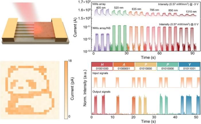
- Record-Low Dark Current: The GaSb/Bi2O₂Se NW/NS and NW array/NS devices achieve ultralow dark currents of 0.07 pA and 0.08 pA, respectively, enabling exceptionally clean signal detection.
- Ultrafast Response: Response times of < 2 ms (single NW/NS) and 6/4 ms (NW array/NS) outperform most comparable systems, crucial for high-speed data processing.
- Broadband Sensitivity: Effective photodetection from visible to 1310 nm wavelengths makes these devices versatile for diverse NIR applications.
- Integrated Functionality: Beyond detection, the devices successfully demonstrated self-powered imaging and optical data transmission.
Innovative Design and Mechanisms
- Mixed-Dimensional Type-II Heterojunction: Combining 1D GaSb NWs and 2D Bi2O2Se NSs yields a built-in electric field (~140 meV) that promotes rapid, bias-free separation of photo-generated carriers.
- Array Architecture for Enhanced Performance: Ordered NW arrays, fabricated via contact printing, provide larger active areas, stronger photocurrents, and improved Ilight/Idark ratios.
- Interface Characterization: Advanced tools such as Kelvin probe force microscopy (KPFM), XRD, and AFM confirm precise band alignment and high-quality heterointerfaces.
Applications and Future Outlook
- Imaging: The team demonstrated single-pixel imaging of a “panda,” highlighting potential for compact NIR cameras.
- Photocommunication: Successful ASCII code transmission (“HAPPY”) proves feasibility for secure, high-speed optical links.
- Next Steps: Scaling up fabrication, integrating with flexible substrates, and exploring other material pairings could open new pathways for wearable sensors, IoT devices, and space-borne imaging systems.
Stay tuned for more exciting developments from Prof. Yang’s group as they continue redefining the boundaries of self-powered optoelectronics and NIR photodetection technology.
Original publication


Other news from the department science


