Diamond as a building material for optical circuits
A revolution in optomechanical materials enables manufacturing of monolithic components
Advertisement


The application of light for information processing opens up a multitude of possibilities. However, to be able to adequately use photons in circuits and sensors, materials need to have particular optical and mechanical properties. Researchers at the Karlsruhe Institute of Technology (KIT) have now for the first time used polycrystalline diamond to manufacture optical circuits and have published their results online in Nature Communications.

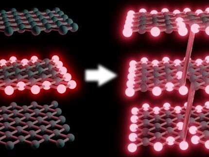
Two parallel free-standing waveguides made of polycrystalline diamond serve as mechanical resonators. Optical fields (red/blue) are observed to propagate inside of them.
KIT/CFN/Pernice
“Diamond has several properties that allow us to manufacture all components of a ready-to-use optomechanical circuit monolithically, so to speak,” says KIT research group leader Wolfram Pernice. “The elements thus manufactured that is, the resonators, circuits, and the wafer, are attractive because of their high quality.”
Diamond is optically transparent to light waves of a wide range of wavelengths including the visible spectrum between 400 and 750 nm. It is due to this fact that it can be used specifically in optomechanical circuits for applications in sensor technology and fluorescence imaging, or for novel optical biological measuring methods. Whereas the high refractive index of diamond and the absence of absorption allow an efficient photon transport, its high modulus of elasticity makes it a robust material which adapts excellently to rough surfaces and releases heat rapidly.

So far, optical circuits have been manufactured using monocrystalline diamond substrates i.e., highly pure crystals with typically no more than one impurity atom to every one billion diamond atoms. Such circuits are bound to be small and their application to optical systems has required sophisticated fabrication methods.
Now, for the first time, the research group headed by Pernice used polycrystalline diamond for the fabrication of wafer-based optomechanical circuits. Even though its crystal structures are more irregular, polycrystalline diamond is robust and thus can be more easily processed. It is due to these specific properties that polycrystalline diamond can be used on much larger areas than monocrystalline material. Polycrystalline diamond conducts photons almost as efficiently as the monocrystalline substrate and is suitable for industrial use. As a matter of fact, monolithic optomechanical components could not have been manufactured without this new material.
Optomechanics combines integrated optics with mechanical elements e.g., with nanomechanical resonators in the case of the optomechanical circuit developed by Pernice and his group. These oscillatory systems react to a certain frequency. When that frequency occurs, the resonator is excited into vibration. “Nanomechanical resonators are among today’s most sensitive sensors and are used in various precision measurements. It is extremely difficult, however, to address such smallest components through conventional measuring methods,” explains Patrik Rath, first author of the study. “In our study, we have made use of the fact that today, nanophotonic components can be manufactured in the same sizes as nanoscale mechanical resonators. When the resonator responds, corresponding optical signals are transferred directly to the circuit.” This novel development has allowed the combining of once separate fields of research and has enabled the realization of highly efficient optomechanical circuits.
Integrated optics works in a similar manner to integrated electrical circuits. Whereas optical circuits transmit information via photons, conventional electronic circuits transfer data via electrons. Integrated optics aims to combine all components required for optical communication in an integrated optical circuit to avoid a detour via electrical signals. In both cases, the respective circuits are applied to slices less than one mm in thickness i.e., to the so-called wafers.
The polycrystalline diamond was manufactured in cooperation with the Fraunhofer Institute for Applied Solid State Physics and the company Diamond Materials in Freiburg, Germany. The prototypes manufactured within the Integrated Quantum Photonics-project at the DFG Center for Functional Nanostructures (CFN) in Karlsruhe open up new ways for entirely optically controlled platforms that are increasingly needed in fundamental research and advanced sensor technologies. These technologies include accelerometers that are integrated in various electronic devices such as airbag sensors or smartphone waterlevels.


Other news from the department science


These products might interest you


Most read news


More news from our other portals


See the theme worlds for related content
Topic world Sensor technology
Sensor technology has revolutionized the chemical industry by providing accurate, timely and reliable data across a wide range of processes. From monitoring critical parameters in production lines to early detection of potential malfunctions or hazards, sensors are the silent sentinels that ensure quality, efficiency and safety.