Researchers develop technique that could open doors to faster nanotech commercialization
An innovative method allows silicon nanowires and carbon nanotubes to grow directly on microstructures in a room temperature chamber
04-Jul-2003
Engineers at the University of California, Berkeley, have found an innovative way to grow silicon nanowires and carbon-nanotubes/order_t/'>carbon nanotubes directly on microstructures in a room temperature chamber, opening the doors to cheaper and faster commercialization of a myriad of nanotechnology-based devices.
The researchers were able to precisely localize the extreme heat necessary for nanowire and nanotube growth, protecting the sensitive microelectronics - which remained at room temperature - just a few micrometers away, or about one-tenth the diameter of a strand of human hair.
The new technique, described in the June 24 online issue of the journal Applied Physics Letters, eliminates cumbersome middle steps in the manufacturing process of sensors that incorporate nanotubes or nanowires. An image of the technique will be featured on the cover of the journal's June 30 print issue.
Such devices would include early-stage disease detectors that could signal the presence of a single virus or an ultra-sensitive biochemical sensor triggered by mere molecules of a toxic agent.
"One very big problem right now is figuring out how to assemble these nanowires or nanotubes onto a microchip in a way that is commercially feasible," said Liwei Lin, associate professor of mechanical engineering at UC Berkeley.
Lin tested the new technique for processing nano-based microelectromechanical systems (MEMS) devices with his graduate students Ongi Englander, lead author of the paper, and Dane Christensen, co-author of the paper.
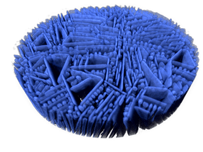
Shown above are oblique and closeup views of silicon nanowire growth. The nanowires are centrally located to 35 micrometers of a 100 micrometer-long microstructure. (Courtesy Bob Prohaska and Ongi Englander)
The steps used in creating nanowires and nanotubes are essentially the same, though different chemicals and temperatures may be used. "It's like a recipe," said Englander. "Different ingredients are used depending upon whether you want to make a chocolate chip muffin or a banana nut muffin, but the steps are more or less the same."
The UC Berkeley researchers, in this case, used a gold-palladium alloy with silane vapor to create silicon nanowires, and a nickel-iron alloy with acetylene vapor to create carbon nanotubes.
The typical nanowire or nanotube production process occurs in a furnace at temperatures of 600 to 1,000 degrees Celsius (1,112 to 1,832 degrees Fahrenheit). The procedure begins with a 1 square centimeter silicon wafer that is coated thinly with a metal alloy. A vapor is then directed towards the substrate, and the metal alloy acts as a catalyst in a chemical reaction that eventually forms billions of nanowire or nanotube precipitates.
The nanomaterials are harvested by being placed in a liquid solvent, such as ethanol, and blasted with ultrasonic waves to loosen them from the wafer surface. Researchers must then sort through the billions of nanowires or nanotubes to find the few that meet the specifications they need for their sensor applications.
Correctly orienting a nanowire onto a 5 square millimeter microchip would be like sticking a sewing needle into a football field with an accuracy of a few micrometers.
"If I had the right pair of tweezers, I could pick out the nanowire that I wanted and manipulate it, but such tweezers don't exist," said Englander.
So instead of finding a way to produce nanomaterials separately and then connecting them to larger scale systems, the researchers decided to grow the silicon nanowires and carbon nanotubes directly onto the circuit board.
The challenge was in protecting the sensitive microelectronics that would melt in the tremendously high temperatures needed to create the nanomaterials.
Resistive heating provided the answer. "It's the same idea as the wires in a toaster," said Englander. "The electrical current flows through the wire to generate the heat."
The researchers passed the current through a wire to the specific locations on the microstructure where they wanted the nanowires or nanotubes to grow. In one experiment, an area was heated to 700 degrees Celsius while another spot just a few micrometers away sat comfortably at 25 degrees Celsius. The entire circuit board was placed in a vacuum chamber for the tests.
"It's the immediate integration of the nanoscale with the microscale," said Christensen, who worked on the carbon nanotube experiments.
The experiments yielded silicon nanowires from 30 to 80 nanometers in diameter and up to 10 micrometers long, and carbon nanotubes that were 10 to 30 nanometers in diameter and up to 5 micrometers long.
"This is a very unique approach," said Lin. "This method allows the production of an entire nano-based sensor in a process similar to creating computer chips. There would be no post-assembly required."
The researchers are continuing experiments to fine-tune the temperatures and length of heating time to create desired lengths of nanowires and nanotubes.
The California State nanotechnology Fellowship and the GAANN Fellowship helped support this research.
Other news from the department science


Get the chemical industry in your inbox
From now on, don't miss a thing: Our newsletter for the chemical industry, analytics, lab technology and process engineering brings you up to date every Tuesday and Thursday. The latest industry news, product highlights and innovations - compact and easy to understand in your inbox. Researched by us so you don't have to.