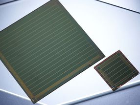
Dow Introduces Industry's First Spin-On Etch Stop Film
Leveraging its expertise in materials science, The Dow Chemical Company today introduced Ensemble ES solution, the industry's first production-ready spin-on etch stop material for advanced semiconductor device production. Ensemble ES solution represents a new class of thin film materials, and builds on Dow's success with SiLK* semiconductor dielectric resin, the leading low-k film for the 130nm technology node and beyond.
Designed for use with SiLK resins, Ensemble ES films give advanced logic IC manufacturers the ability to reduce the effective dielectric constant (k) of device structures, resulting in faster, cheaper and more powerful chips. "A key advantage of our Ensemble ES formulation is that it has been engineered to be compatible with the entire product line for SiLK resins so that our customers achieve good adhesion and film quality for both the etch stop and the overlaying SiLK films," said Mark McClear, business director for Dow's Semiconductor Fab Materials group.
Ensemble ES solution, an organosilane-based spin-on polymer, offers a k value of <3.2, compared to ~5.0 for competing etch stops applied by chemical vapor deposition (CVD) methods. When used in combination with advanced SiLK semiconductor dielectric resins, which offer k values as low as 2.0, Ensemble ES films enable chipmakers to lower the effective k value of the dielectric stack and reduce cost of ownership. "As the semiconductor industry rapidly moves toward production of devices in the 130nm technology node, chipmakers require a low cost-of-ownership path to integrating low-k films while continuing to improve device performances," said McClear. "Unlike conventional CVD-applied etch stops, Ensemble ES solution is deposited with the same spin-on tool as our industry-leading SiLK dielectric resin. By avoiding the transfer from the spin-on track to the CVD chamber, chipmakers benefit from improved throughput and lower cost of ownership."
Another critical performance criteria for these etch stop films is etch selectivity. With an etch selectivity of greater than 20:1, Ensemble ES films show etch performance which is more than twice that of competing films. This allows thinner etch stop films to be used and results in further reductions in the effective dielectric constant of the stack.
"As part of our commitment to ensure smooth integration schemes for device production using SiLK resins, Dow is developing a full family of spin-on hardmask materials for applications throughout the dielectric stack - including etch stops, CMP stops, top hardmasks and copper barrier layers," McClear said. "Our intention is to enable chipmakers to process the entire dielectric stack on a single tool: the spin track." The Ensemble ES layer is the first step toward a complete spin-on dielectric stack and is designed to simplify the integration of SiLK resins into manufacturing flows. Other layers are expected to become available for beta evaluations beginning in 2002.
Members of the SiLKnet Alliance – an industry-wide collaboration of tool and materials suppliers to streamline fab processes for SiLK resins – have begun developing integration strategies for Ensemble ES solution. Sample Ensemble ES films will be available to beta customers for module development in the fourth quarter of 2001; Dow expects to begin commercial production in the first quarter of 2002.
About SiLK Semiconductor Dielectric Resin SiLK resins are a family of spin-on, low-k ILD materials that allow semiconductor manufacturers to increase the speed and performance of their chips by enabling denser circuitry. First generation SiLK resin products offer k=2.6 for both copper damascene and aluminum/tungsten processing. Dow also offers a clear path to next-generation chip technologies with porous SiLK resin (k=2.0), which is being developed for 100nm chip designs.

Other news from the department research and development


Get the chemical industry in your inbox
From now on, don't miss a thing: Our newsletter for the chemical industry, analytics, lab technology and process engineering brings you up to date every Tuesday and Thursday. The latest industry news, product highlights and innovations - compact and easy to understand in your inbox. Researched by us so you don't have to.