Unique X-ray Topography Based Defect Characterization for SiC Wafers Honored with Georg Waeber Innovation Award 2023
Advertisement


A cross-organizational team from Rigaku SE and Fraunhofer IISB has established a new semiconductor material characterization method in their jointly operated Center of Expertise for x-ray topography in Erlangen, Germany. They succeeded not only in developing an industry-ready X-ray topography system, but also in employing defect detection and quantification algorithms, achieving a worldwide unique material characterization method for silicon carbide (SiC) wafers. SiC is an excellent semiconductor for application areas like electric mobility and transportation, sustainable energy supply, industrial infrastructure up to sensors and quantum technologies even under harsh operating conditions. As representatives for the whole research team, Dr. Kranert and Dr. Reimann from Fraunhofer IISB and Dr. Hippler, Managing Director Rigaku Europe SE, have won the Georg Waeber Innovation Award 2023 from the Förderkreis für die Mikroelektronik e.V. (Microelectronics Promotion Society).
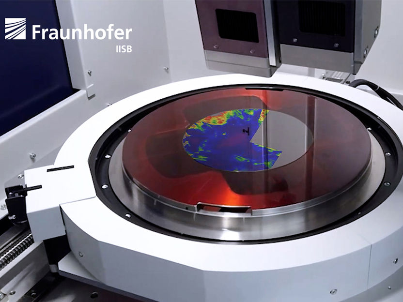
In-tool view of the Rigaku XRTmicron with animated defect map to showcase the non-destructive, high-speed metrology process across the entire wafer surface.
© Elisabeth Iglhaut / Fraunhofer IISB
Pioneering holistic material defect characterization with X-ray topography
In 2021, Rigaku SE and Fraunhofer IISB have founded the Center of Expertise for X-ray Topography, a joint lab that is located at the IISB’s headquarters in Erlangen, Germany. Here, the cross-organizational team has now developed a new metrology that is non-destructive, robust, reliable, high-throughput and therefore capable of swiftly detecting all relevant crystallographic defects in SiC substrates. For the first time worldwirde, this innovation realized the holistic approach of setting up the measurement device, i.e., the X-ray topography (XRT) tool as well as formulating appropriate measurement and analysis routines that specifically meet the industry’s demands for speed, reliability, and accuracy. The development process was supported by rigorous scientific validation of the results, a crucial factor for the acceptance of a new approach in the industry.
Until now, no such industry-ready metrology existed for the early stages of SiC power electronics manufacturing, especially at substrate or crystal (commonly referred to as the “puck”) level. This breakthrough in SiC substrate inspection makes it no longer necessary to, e.g., destructively defect etch and discard semiconductor substrates for characterization, as is currently often the case. In consequence, the developed XRT metrology is superior to these existing substrate characterization methods employed in the industry, ultimately leading to substantial cost savings.
Effectively, this technology, developed in Germany, provides everything needed to become the industry standard for specifying and controlling substrate quality in production as well as for R&D substrate and device manufacturers worldwide. The success of this joint innovation is vividly illustrated by the new business, which Rigaku has successfully established in less than two years. Now, the Japan-based company is the world's leading supplier of XRT tools for SiC substrate and device manufacturing.
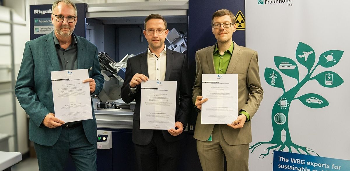
The innovative metrology approach has been driven significantly by Dr. Michael Hippler, Managing Director of Rigaku Europe SE, and Dr. Christian Kranert with Dr. Christian Reimann, both group managers in the Fraunhofer IISB’s Materials department. Hence the scientists were selected for the Georg Waeber Innovation Award 2023 by the Förderkreis für die Mikroelektronik e.V. (Microelectronics Promotion Society). The Förderkreis is an association of industry companies, two Fraunhofer institutes, four chairs of the University of Erlangen-Nuremberg and the Nuremberg Chamber of Commerce and Industry. The main objective is to foster a smooth exchange between science and industry, which is manifested in the Georg Waeber Innovation Award. The award is presented annually for outstanding scientific achievements and places a strong emphasis on the advancement of knowledge in microelectronics and its practical application in the industry. On October 25, 2023, Dr. Hippler, Dr. Reimann and Dr. Kranert received the award during a ceremony at Fraunhofer IISB in Erlangen.
Paving the way for the next generation of SiC power electronics
SiC semiconductor devices play a pivotal role in the power electronics industry. As a replacement for conventional silicon-based power electronics, SiC has the potential to enhance energy efficiency while reducing system costs. It is relevant across various application areas from electric mobility and transportation, sustainable energy supply, industrial infrastructure up to sensors and quantum technologies even under harsh operating conditions. Consequently, processing low-cost, energy-efficient, and highly reliable SiC power devices is a critical endeavor with the worldwide electrification trend. The production capacities for SiC wafers experience significant growth, which goes hand in hand with an increasing demand for wafer inspection and metrology within the SiC industry. In particular, manufacturers of substrates and power devices require precice information regarding the quality of substrates in terms of crystallographic defects, their distribution across the entire wafer area, and absolute quantities.


Other news from the department science


