To use all functions of this page, please activate cookies in your browser.
My watch list
my.chemeurope.com
my.chemeurope.com
With an accout for my.chemeurope.com you can always see everything at a glance – and you can configure your own website and individual newsletter.
- My watch list
- My saved searches
- My saved topics
- My newsletter
DislocationIn materials science, a dislocation is a crystallographic defect, or irregularity, within a crystal structure. The presence of dislocations strongly influences many of the properties of materials. The theory was originally developed by Vito Volterra in 1905. Some types of dislocations can be visualised as being caused by the termination of a plane of atoms in the middle of a crystal. In such a case, the surrounding planes are not straight, but instead bend around the edge of the terminating plane so that the crystal structure is perfectly ordered on either side. The analogy with a stack of paper is apt: if a half a piece of paper is inserted in a stack of paper, the defect in the stack is only noticeable at the edge of the half sheet. There are two primary types: edge dislocations and screw dislocations. Mixed dislocations are intermediate between these.
Mathematically, dislocations are a type of topological defect, sometimes called a soliton. The mathematical theory explains why dislocations behave as stable particles: they can be moved about, but maintain their identity as they move. Two dislocations of opposite orientation, when brought together, can cancel each other (this is the process of annihilation), but a single dislocation typically cannot "disappear" on its own. Product highlight
Dislocation geometry
There are two main types of dislocation, edge and screw. Dislocations found in real materials typically are mixed, meaning that they have characteristics of both. A crystalline material consists of a regular array of atoms, arranged into e planes (imagine stacking oranges in a grocers, each of the trays of oranges are the lattice planes). One approach is to begin by considering a 3-d representation of a perfect crystal lattice, with the atoms represented by spheres. The viewer may then start to simplify the representation by visualising planes of atoms instead of the atoms themselves (Figure A).
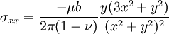
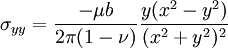
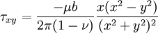
Edge dislocationsAn edge dislocation is a defect where an extra half-plane of atoms is introduced mid way through the crystal, distorting nearby planes of atoms. A simple schematic diagram of such atomic planes can be used to illustrate lattice defects such as dislocations. (Figure B represents the "extra half-plane" concept of an edge type dislocation). The dislocation has two properties, a line direction, which is the direction running along the bottom of the extra half plane, and the Burgers vector which describes the magnitude and direction of distortion to the lattice. In an edge dislocation, the Burgers vector is perpendicular to the line direction. The stresses caused by an edge dislocation are complex due to its inherent asymmetry. These stresses are described by three equations:[1]
where μ is the shear modulus of the material, b is the Burgers vector, ν is Poisson's ratio and x and y are coordinates. These equations suggest a vertically oriented dumbbell of stresses surrounding the dislocation, with compression experienced by the atoms near the "extra" plane, and tension experienced by those atoms near the "missing" plane.[2] Screw dislocations
A screw dislocation is much harder to visualize. Imagine cutting a crystal along a plane and slipping one half across the other by a lattice vector, the halves will fit back together without leaving a defect. If the cut only goes part way though the crystal, and then slipped, the boundary of the cut is a screw dislocation. It comprises a structure in which a helical path is traced around the linear defect (dislocation line) by the atomic planes in the crystal lattice (Figure C). In pure screw dislocations, the Burgers vector is parallel to the line direction. Despite the difficulty in visualization, the stresses caused by a screw dislocation are less complex than those of an edge dislocation. These stresses need only one equation, as symmetry allows only one radial coordinate to be used:[3]
where μ is the shear modulus of the material, b is the Burgers vector, and r is a radial coordinate. This equation suggests a long cylinder of stress radiating outward from the cylinder and decreasing with distance. Please note, this simple model results in an infinite value for the core of the dislocation at r=0 and so it is only valid for stresses outside of the core of the dislocation.[4] Mixed dislocationsIn many materials, dislocations are found where the line direction and Burgers vector are neither perpendicular nor parallel and these dislocations are called mixed dislocations, consisting of both screw and edge character. Observation of DislocationsWhen a dislocation line intersects the surface of a metallic material, the associated strain field locally increases the relative susceptibility of the material to acidic etching and an etch pit of regular geometrical format results. If the material is strained (deformed) and repeatedly re-etched, a series of etch pits can be produced which effectively trace the movement of the dislocation in question. Transmission electron microscopy can be used to observe dislocations within the microstructure of the material. Thin foils of metallic samples are prepared to render them transparent to the electron beam of the microscope. The electron beam suffers diffraction by the regular crystal lattice planes of the metal atoms and the differing relative angles between the beam and the lattice planes of each grain in the metal's microstructure result in image contrast (between grains of different crystallographic orientation). The less regular atomic structures of the grain boundaries and in the strain fields around dislocation lines have different diffractive properties than the regular lattice within the grains, and therefore present different contrast effects in the electron micrographs. (The dislocations are seen as dark lines in the lighter, central region of the micrographs on the right). Transmission electron micrographs of dislocations typically utilize magnifications of 50,000 to 300,000 times (though the equipment itself offers a wider range of magnifications than this). Some microscopes also permit the in-situ heating and/or deformation of samples, thereby permitting the direct observation of dislocation movement and their interactions. Note the characteristic 'wiggly' contrast of the dislocation lines as they pass through the thickness of the material. Note also that a dislocation cannot end within a crystal; the dislocation lines in these images end at the sample surface. A dislocation can only be contained within a crystal as a complete loop. Field ion microscopy and atom probe techniques offer methods of producing much higher magnifications (typically 3 million times and above) and permit the observation of dislocations at an atomic level. Where surface relief can be resolved to the level of an atomic step, screw dislocations appear as distinctive spiral features - thus revealing an important mechanism of crystal growth: where there is a surface step, atoms can more easily add to the crystal, and the surface step associated with a screw dislocation is never destroyed no matter how many atoms are added to it. (By contrast, traditional optical microscopy, which is not appropriate for the observation of dislocations, typically offers magnifications up to a maximum of only around 2000 times). After chemical etching, small pits are formed where the etching solution preferentially attacks the more highly strained material around the dislocations. Thus, the image features indicate points at which dislocations intercept the sample surface. In this way, dislocations in silicon, for example, can be observed indirectly using an interference microscope. Crystal orientation can be determined by the shape of dislocations - 100 elliptical, 111 - triangular (pyramidal). Sources of DislocationsDislocation density in a material can be increased by plastic deformation by the following relationship: The creation of a dislocation by homogeneous nucleation is a result of the rupture of the atomic bonds along a line in the lattice. A plane in the lattice is sheared, resulting in 2 oppositely faced half planes or dislocations. These dislocations move away from each other through the lattice. Since homogeneous nucleation forms dislocations from perfect crystals and requires the simultaneous breaking of many bonds, the energy required for homogeneous nucleation is high. For instance the stress required for homogeneous nucleation in copper has been shown to be Irregularities at the grain boundaries in materials can produce dislocations which propagate into the grain. The steps and ledges at the grain boundary are an important source of dislocations in the early stages of plastic deformation. The surface of a crystal can produce dislocations in the crystal. Due to the small steps on the surface of most crystals, stress in certain regions on the surface is much larger than the average stress in the lattice. The dislocations are then propagated into the lattice in the same manner as in grain boundary initiation. In monocrystals, the majority of dislocations are formed at the surface. The dislocation density 200 micrometres into the surface of a material has been shown to be six times higher than the density in the bulk. However, in polycrystalline materials the surface sources cannot have a major effect because most grains are not in contact with the surface. The interface between a metal and an oxide can greatly increase the number of dislocations created. The oxide layer puts the surface of the metal in tension because the oxygen atoms squeeze into the lattice, and the oxygen atoms are under compression. This greatly increases the stress on the surface of the metal and consequently the amount of dislocations formed at the surface. The increased amount of stress on the surface steps results in an increase of dislocations.[5] Dislocations, slip and plasticityUntil the 1930s, one of the enduring challenges of materials science was to explain plasticity in microscopic terms. A naive attempt to calculate the shear stress at which neighbouring atomic planes slip over each other in a perfect crystal suggests that, for a material with shear modulus G, shear strength τm is given approximately by:
As shear modulus in metals is typically within the range 20 000 to 150 000 MPa, this is difficult to reconcile with shear stresses in the range 0.5 to 10 MPa observed to produce plastic deformation in experiments. In 1934, Egon Orowan, Michael Polanyi and G. I. Taylor, roughly simultaneously, realized that plastic deformation could be explained in terms of the theory of dislocations. Dislocations can move if the atoms from one of the surrounding planes break their bonds and rebond with the atoms at the terminating edge. In effect, a half plane of atoms is moved in response to shear stress by breaking and reforming a line of bonds, one (or a few) at a time. The energy required to break a single bond is far less than that required to break all the bonds on an entire plane of atoms at once. Even this simple model of the force required to move a dislocation shows that plasticity is possible at much lower stresses than in a perfect crystal. In many materials, particularly ductile materials, dislocations are the "carrier" of plastic deformation, and the energy required to move them is less than the energy required to fracture the material. Dislocations give rise to the characteristic malleability of metals. When metals are subjected to "cold working" (deformation at temperatures which are relatively low as compared to the material's absolute melting temperature, Tm, i.e., typically less than 0.3 Tm) the dislocation density increases due to the formation of new dislocations and dislocation multiplication. The consequent increasing overlap between the strain fields of adjacent dislocations gradually increases the resistance to further dislocation motion. This causes a hardening of the metal as deformation progresses. This effect is known as strain hardening (also “work hardening”). Tangles of dislocations are found at the early stage of deformation and appear as non well-defined boundaries; the process of dynamic recovery leads eventually to the formation of a cellular structure containing boundaries with misorientation lower than 15° (low angle grain boundaries). In addition, adding pinning points that inhibit the motion of dislocations, such as alloying elements, can introduce stress fields that ultimately strengthen the material by requiring a higher applied stress to overcome the pinning stress and continue dislocation motion. The effects of strain hardening by accumulation of dislocations and the grain structure formed at high strain can be removed by appropriate heat treatment (annealing) which promotes the recovery and subsequent recrystallisation of the material. The combined processing techniques of work hardening and annealing allow for control over dislocation density, the degree of dislocation entanglement, and ultimately the yield strength of the material. Dislocation ClimbDislocations can slip in planes containing both the dislocation and the Burgers Vector. For a screw dislocation, the dislocation and the Burgers vector are parallel, so the dislocation may slip in any plane containing the dislocation. For an edge dislocation, the dislocation and the Burgers vector are perpendicular, so there is only one plane in which the dislocation can slip. There is an alternative mechanism of dislocation motion, fundamentally different from slip, that allows an edge dislocation to move out of its slip plane, known as dislocation climb. Dislocation climb allows an edge dislocation to move perpendicular to its slip plane. The driving force for dislocation climb is the movement of vacancies through a crystal lattice. If a vacancy moves next to the boundary of the extra half plane of atoms that forms an edge dislocation, the atom in the half plane closest to the vacancy can "jump" and fill the vacancy. This atom shift "moves" the vacancy in line with the half plane of atoms, causing a shift, or positive climb, of the dislocation. The process of a vacancy being absorbed at the boundary of a half plane of atoms, rather than created, is known as negative climb. Since dislocation climb results from individual atoms "jumping" into vacancies, climb occurs in single atom diameter increments. During positive climb, the crystal shrinks in the direction perpendicular to the extra half plane of atoms because atoms are being removed from the half plane. Since negative climb involves an addition of atoms to the half plane, the crystal grows in the direction perpendicular to the half plane. Therefore, compressive stress in the direction perpendicular to the half plane promotes positive climb, while tensile stress promotes negative climb. This is one main difference between slip and climb, since slip is caused by only shear stress. One additional difference between dislocation slip and climb is the temperature dependence. Climb occurs much more rapidly at high temperatures than low temperatures due to an increase in vacancy motion. Slip, on the other hand, has only a small dependence on temperature. Notes
Bibliography
|
|
| This article is licensed under the GNU Free Documentation License. It uses material from the Wikipedia article "Dislocation". A list of authors is available in Wikipedia. |


 . Since the dislocation density increases with plastic deformation, a mechanism for the creation of dislocations must be activated in the material. Three mechanisms for dislocation formation are formed by homogeneous nucleation, grain boundary initiation, and interfaces the lattice and the surface, precipitates, dispersed phases, or reinforcing fibers.
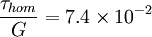 , where G is the shear modulus of copper (46 GPa). Solving for
Last viewed


