To use all functions of this page, please activate cookies in your browser.
My watch list
my.chemeurope.com
my.chemeurope.com
With an accout for my.chemeurope.com you can always see everything at a glance – and you can configure your own website and individual newsletter.
- My watch list
- My saved searches
- My saved topics
- My newsletter
Electron mobilityProduct highlight
Electron MobilityIn physics, electron mobility (or simply, mobility), is a quantity relating the drift velocity of electrons to the applied electric field across a material, according to the formula:
where
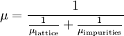
It is the application for electrons of the more general phenomenon of electrical mobility of charged particles in a fluid under an applied electric field. In semiconductors, mobility can also apply to holes as well as electrons. Conceptual overviewIn a solid, electrons (and in the case of semiconductors, holes) will move around randomly in the absence of an applied electric field. Therefore, if one averages the movement over time there will be no overall motion of charge carriers in any particular direction. However upon applying an electric field, electrons will be accelerated in an opposite direction to the electric field. The summation of the time between acceleration of electrons due to electric field and deceleration of electrons due to collisions and lattice scattering events (caused by phonons, crystal defects, impurities, etc.) over the mean free path between scattering events results in the electrons having an average drift velocity. This net electron motion must be orders of magnitude less than the normally occurring random motion, otherwise the mobility equation is not valid (i.e., typical drift speeds in copper being of the order of 10-4 m·s−1 compared to the speed of random electron motion of 105 m·s−1). In a semiconductor the two charge carriers, electrons and holes, will typically have different drift velocities for the same electric field. In a plasma there is analogous behavior with ions and free electrons. In a vacuum, electrons will accelerate non-stop in an electric field according to Newton's second law of motion. This is known as "ballistic transport". Thus electron mobility is undefined for electronic movement in a vacuum. In a solid, if the electrons must move only a very short distance (distance comparable with the Brownian motion), quasi-ballistic transport is possible. In SI units, mobility is normally measured in m2/(V·s). Since mobility is usually a strong function of material impurities and temperature, and is determined empirically, mobility values are typically presented in table or chart form. Mobility is also different for electrons and holes in a semiconductor. An approximation of the mobility function can be written as a combination of influences from lattice vibrations (phonons) and from impurities by the Matthiessen's Rule:
Mobility in gas phaseMobility is defined for any species in the gas phase, encountered mostly in plasma physics and is defined as:
where
Mobility is related to the species' diffusion coefficient
where
But both the momentum transfer mean free path and the momentum transfer collision frequency are difficult to calculate. Many other mean free paths can be defined. In the gas phase,
When
where
Mobility at the silicon dioxide / silicon interface of MOSFET transistorsFor n-channel or p-channel MOSFETs, the electron or hole mobility at the silicon dioxide / silicon interface has a very strong effect on the speed of the device. In 1997, Professor Mark Lundstrom of Purdue University pointed out for nanotransistors, quasi-ballistic transport is possible and maximum charge carrier speed is controlled by mobility (instead of by velocity saturation according to conventional theory)[1]. Increasing the mobility of MOSFETs can have a profound benefit to digital electronics, thus all major digital semiconductor manufacturers have been exploring methods to increase mobility at the silicon dioxide / silicon interface of MOS transistors. One important approach is known as strain engineering. Usually, three scattering mechanisms are present at the silicon dioxide / silicon interface of MOS transistors:
Recently, scientists have been studying the possibility of "remote Coulombic scattering", which is also known as "remote charge scattering"[2]. Remote charge scattering can come from two sources:
In 2005, W.S. Lau pointed out as Lau's hypothesis that "remote Coulombic scattering" is only important in the subthreshold region and in the region slightly above threshold.[3]. ExamplesTypical electron mobility for Si at room temperature (300 K) is 0.92 m2/(V·s) References
See alsoCategories: Semiconductors | Plasma physics |
|
| This article is licensed under the GNU Free Documentation License. It uses material from the Wikipedia article "Electron_mobility". A list of authors is available in Wikipedia. |


 is the drift velocity
 is the applied electric field
 is the mobility
 .
.

 is the charge of the species,
 is the momentum transfer collision frequency, and
 is the mass.
 through an exact (thermodynamically required) equation known as the
  ,
,
 is the
  is the
  .
.
 is often defined as the diffusional mean free path, by assuming a simple approximate relation is exact:
 .
.
 is the root mean square speed of the gas molecules:


