To use all functions of this page, please activate cookies in your browser.
My watch list
my.chemeurope.com
my.chemeurope.com
With an accout for my.chemeurope.com you can always see everything at a glance – and you can configure your own website and individual newsletter.
- My watch list
- My saved searches
- My saved topics
- My newsletter
Photolithography
Photolithography resembles the conventional lithography used in printing, and shares some fundamental principles with photography. It is used because it affords exact control over the shape and size of the objects it creates, and because it can create patterns over an entire surface simultaneously. Its main disadvantages are that it requires a flat substrate to start with, it is not very effective at creating shapes that are not flat, and it can require extremely clean operating conditions. Product highlight
Basic procedure
A single iteration of photolithography combines several steps in sequence. Modern cleanrooms use automated, robotic wafertrack systems to coordinate the process. The procedure described here omits some advanced treatments, such as thinning agents or edge-bead removal. [1] PreparationThe wafer is initially heated to a temperature sufficient to drive off any moisture that may be present on the wafer surface. Wafers that have been in storage must be chemically cleaned to remove contamination. A liquid or gaseous "adhesion promoter", such as hexamethyldisilazane (HMDS), is applied to promote adhesion of the photoresist to the wafer. Photoresist applicationThe wafer is covered with photoresist ("PR") by spin coating. A viscous, liquid solution of photoresist is dispensed onto the wafer, and the wafer is spun rapidly to produce a uniformly thick layer. The spin coating typically runs at 1200 to 4800 rpm for 30 to 60 seconds, and produces a layer between 2.5 and 0.5 micrometres thick. The photoresist-coated wafer is then "soft-baked" or "prebaked" to drive off excess solvent, typically at 90 to 100 °C for 5 to 30 minutes.[citation needed] Sometimes a nitrogen atmosphere is used. Exposure and developingAfter prebaking, the photoresist is exposed to a pattern of intense light. Optical lithography typically uses ultraviolet light (see below). Positive photoresist, the most common type, becomes less chemically robust when exposed; negative photoresist becomes more robust. This chemical change allows some of the photoresist to be removed by a special solution, called "developer" by analogy with photographic developer. A post-exposure bake is performed before developing, typically to help reduce standing wave phenomena caused by the destructive and constructive interference patterns of the incident light. The develop chemistry is delivered on a spinner, much like photoresist. Developers originally often contained sodium hydroxide (NaOH). However, sodium is considered an extremely undesirable contaminant in MOSFET fabrication because it degrades the insulating properties of gate oxides. Metal-ion-free developers such as tetramethylammonium hydroxide (TMAH) are now used. The resulting wafer is then "hard-baked", typically at 120 to 180 °C[citation needed] for 20 to 30 minutes. The hard bake solidifies the remaining photoresist, to make a more durable protecting layer in future ion implantation, wet chemical etching, or plasma etching. EtchingIn the etching step, a liquid ("wet") or plasma ("dry") chemical agent removes the uppermost layer of the substrate in the areas that are not protected by photoresist. In semiconductor fabrication, dry etching techniques are generally used, as they can be made anisotropic, in order to avoid significant undercutting of the photoresist pattern. This is essential when the width of the features to be defined is similar to or less than the thickness of the material being etched (ie when the aspect ratio approaches unity). Wet etch processes are generally isotropic in nature, which is often indispensable for microelectromechanical systems (MEMS), where suspended structures must be "released" from the underlying layer. The development of low-defectivity anisotropic dry-etch process has enabled the ever-smaller features defined photolithographically in the resist to be transferresd to the substrate material. Photoresist removalAfter a photoresist is no longer needed, it must be removed from the substrate. This usually requires a liquid "resist stripper", which chemically alters the resist so that it no longer adheres to the substrate. Alternatively, photoresist may be removed by a plasma containing oxygen, which oxidizes it. This process is called ashing, and resembles dry etching. Exposure ("printing") systems
Exposure systems typically produce an image on the wafer using a photomask. The light shines through the photomask, which blocks it in some areas and lets it pass in others. (Maskless lithography projects a precise beam directly onto the wafer without using a mask, but it is not widely used in commercial processes.) Exposure systems may be classified by the optics that transfer the image from the mask to the wafer. Contact and proximityA contact printer, the simplest exposure system, puts a photomask in direct contact with the wafer and exposes it to a uniform light. A proximity printer puts a small gap between the photomask and wafer. In both cases, the mask covers the entire wafer, and simultaneously patterns every die. Contact printing is liable to damage both the mask and the wafer, and this was the primary reason it was abandoned for high volume production. Both contact and proximity lithography require the light intensity to be uniform across an entire wafer, and the mask to align precisely to features already on the wafer. As modern processes use increasingly large wafers, these conditions become increasingly difficult. Research and prototyping processes often use contact lithography, because it uses inexpensive hardware and can achieve high optical resolution. The resolution is approximately the square root of the product of the wavelength and the gap distance. Hence, contact printing offers the best resolution, because its gap distance is approximately zero (neglecting the thickness of the photoresist itself). In addition, nanoimprint lithography may revive interest in this familiar technique, especially since the cost of ownership is expected to be low. Projection
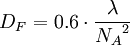
Very-large-scale integration lithography uses projection systems. Unlike contact or proximity masks, which cover an entire wafer, projection masks (also called "reticles") show only one die. Projection exposure systems (steppers) project the mask onto the wafer many times to create the complete pattern. PhotomasksThe image for the mask originates from a computerized data file. This data file is converted to a series of polygons and written onto a square fused quartz substrate covered with a layer of chrome using a photolithographic process. A beam of electrons is used to expose the pattern defined in the data file and travels over the surface of the substrate in either a vector or raster scan manner. Where the photoresist on the mask is exposed, the chrome can be etched away, leaving a clear path for the light in the stepper/scanner systems to travel through. Resolution in projection systemsThe ability to project a clear image of a small feature onto the wafer is limited by the wavelength of the light that is used, and the ability of the reduction lens system to capture enough diffraction orders from the illuminated mask. Current state-of-the-art photolithography tools use deep ultraviolet (DUV) light with wavelengths of 248 and 193 nm, which allow minimum feature sizes down to 50 nm. The minimum feature size that a projection system can print is given approximately by: where
According to this equation, minimum feature sizes can be decreased by decreasing the wavelength, and increasing the numerical aperture, i.e. making lenses larger and bringing them closer to the wafer. However, this design method runs into a competing constraint. In modern systems, the depth of focus is also a concern: The depth of focus restricts the thickness of the photoresist and the depth of the topography on the wafer. Chemical mechanical polishing is often used to flatten topography before high-resolution lithographic steps. Light sourcesHistorically, photolithography has used ultraviolet light from gas-discharge lamps using mercury, sometimes in combination with noble gases such as xenon. These lamps produce light across a broad spectrum with several strong peaks in the ultraviolet range. This spectrum is filtered to select a single spectral line, usually the "g-line" (436 nm) or "i-line" (365 nm). More recently, lithography has moved to "deep ultraviolet", produced by excimer lasers. (In lithography, wavelengths below 300 nm are called "deep UV".) Krypton fluoride produces a 248-nm spectral line, and argon fluoride a 193-nm line. Optical lithography can be extended to feature sizes below 50 nm using 193 nm and liquid immersion techniques. Also termed immersion lithography, this enables the use of optics with numerical apertures exceeding 1.0. The liquid used is typically ultra-pure, deionised water, which provides for a refractive index above that of the usual air gap between the lens and the wafer surface. This is continually circulated to eliminate thermally-induced distortions. Water will only allow NA's of up to ~1.4, but materials with higher refractive indices will allow the effective NA to be increased further. Tools using 157 nm wavelength DUV in a manner similar to current exposure systems have been developed. These were once targeted to succeed 193 nm at the 65 nm feature size node but have now all but been eliminated by the introduction of immersion lithography. This was due to persistent technical problems with the 157 nm technology and economic considerations that provided strong incentives for the continued use of 193 nm technology. High-index immersion lithography is the newest extension of 193 nm lithography to be considered. In 2006, features less than 30 nm were demonstrated by IBM using this technique[2]. Experimental methods
Photolithography has been defeating predictions of its demise for many years. For instance, it was predicted that features smaller than 1 micrometre could not be printed optically. Modern techniques already print features several times smaller than the wavelength of light used - an amazing optical feat. Current research is exploring new tricks in the ultraviolet regime, as well as alternatives to conventional UV, such as electron beam lithography, X-ray lithography, extreme ultraviolet lithography, and immersion lithography. See also
References |
|||
| This article is licensed under the GNU Free Documentation License. It uses material from the Wikipedia article "Photolithography". A list of authors is available in Wikipedia. |


 is the minimum feature size
 is a coefficient that encapsulates process-related factors, and typically equals 0.5
 is the wavelength of light used
 is the numerical aperture of the lens as seen from the wafer