Cost-efficient production process and homogeneous luminosity for OLEDs thanks to micro-scale conductor paths
Advertisement
The trend in lighting technology is towards the large-area and decorative illumination made possible by organic light-emitting diodes (OLEDs). Analysts at NanoMarkets forecast a worldwide market volume of over $2.9 billion for 2012, with sales increasing to around $5.9 billion by 2014. The lighting industry is now looking for economic production techniques for organic lighting. In cooperation with Philips, the Fraunhofer Institute for Laser Technology ILT is developing an cost-efficient process for applying conductor paths to OLEDs.
Organic light-emitting diodes are highly efficient light sources based on organic materials. They achieve high luminous intensity while consuming little energy. OLEDs consist of one or several active organic layers which are energized by two large-area electrodes. The initiated current flow leads to electron-hole recombinations in the organic layer. This produces photons which radiate into the half-space through the conductive, transparent anode - consisting of indium tin oxide (ITO) or similar materials. To distribute the electrical energy evenly over the entire surface of the OLEDs, metallic conductor paths are applied to the ITO layer. The size of the conductor paths plays an important role here: if they are too wide the paths can affect the luminous homogeneity of the light source. In addition to reducing manufacturing costs for OLEDs, the lighting industry is also very keen to produce tiny geometries. A process is required with which narrow metallic conductor paths can be produced efficiently, resulting in savings of energy and resources.
Up to now the metallic conductor material has been applied to the surface of the OLEDs in an energy-intensive high-vacuum sputter process, in which an atomic layer is deposited over the entire surface of the substrate in a high vacuum and removed again using a photolithographic method in the areas where the conductor paths are not required. This subtractive process is very expensive owing to the effort involved in applying and then removing the metal layer not required, which involves a material loss of up to 90%. Furthermore, the photolithographic removal process is environmentally detrimental as the etching solution containing metals has to be disposed of after use. The conventionally produced conductor paths have a width of up to 120 µm and are therefore optically disruptive to the homogeneous luminosity of the OLEDs.
Additive process will reduce costs and the burden on the environment
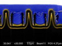
The Fraunhofer ILT is now developing a laser technique to apply micro-scale conductor paths for the industrial partner Philips. A mask foil is placed on the surface of the conductor which represents the negative to the conductor path geometry later required. This is then covered by a donor foil whose material will constitute the conductor path, for example aluminum or copper. The assembly is fixed in place and hit with laser radiation traveling at a speed of up to 2.5 m/s along the mask geometry. A mixture of melt drops and vapor forms, which is transferred from the donor foil to the substrate. The solidified mixture produces the conductor path, whose geometry is determined by the mask. As the process takes place in the ambient atmosphere an expensive process chamber is not required. There is no material loss because the residual material of the donor foil can be re-used.
"This enables us to produce narrow metallic paths with adjustable widths between 40 and 100 µm. They exhibit variable thicknesses between 3 and 15 µm and a resistance of < 0.05 W/sq, so that the electrons are distributed optimally over the entire surface. Our aim is to produce homogeneous luminosity over the entire surface with the new technique," explains Christian Vedder, who is in charge of the project at the Fraunhofer ILT. This manufacturing process also adds greater flexibility in how the layer is configured. Holger Schwab, Project Manager OLED Lighting at Philips, regards cost-efficiency as the main advantage to be gained from the additive laser technique: "This process can considerably reduce the cost of producing OLEDs. The key factors are that almost 100% of the material is utilized and no structuring processes are needed." Conductor paths are used wherever electrical energy needs to be conducted over non-conductive surfaces made of glass, silicon or other materials. Further applications derive from the innovative process, including heated windows in cars and other vehicles as well the production of semiconductors for use in solar cells. Considerable demand exists in these sectors for micro-scale conductor paths because wide conductor paths restrict vision in motor vehicles and cause shading which reduces the efficiency of photovoltaic systems.


