Scientists observe nanowires as they grow
X-ray experiments reveal exact details of self-catalysed growth for the first time
Advertisement


At DESY's X-ray source PETRA III, scientists have followed the growth of tiny wires of gallium arsenide live. Their observations reveal exact details of the growth process responsible for the evolving shape and crystal structure of the crystalline nanowires. The findings also provide new approaches to tailoring nanowires with desired properties for specific applications. The scientists, headed by Philipp Schroth of the University of Siegen and the Karlsruhe Institute of Technology (KIT), present their findings in the journal Nano Letters. The semiconductor gallium arsenide (GaAs) is widely used, for instance in infrared remote controls, the high-frequency components of mobile phones and for converting electrical signals into light for fibre optical transmission, as well as in solar panels for deployment in spacecraft.
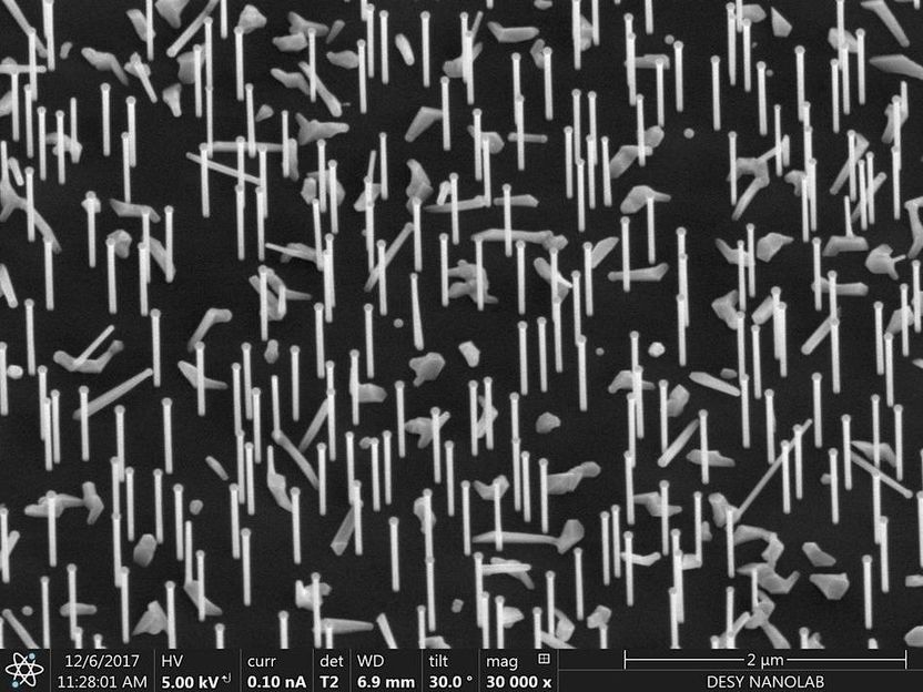
Nano forest: 'Aerial' view of the tiny wires growing on a silicon wafer, captured with a scanning electron microscope at the DESY NanoLab.
DESY, Satishkumar Kulkarni/Thomas Keller
To fabricate the wires, the scientists employed a procedure known as the self-catalysed Vapour-Liquid-Solid (VLS) method, in which tiny droplets of liquid gallium are first deposited on a silicon crystal at a temperature of around 600 degrees Celsius. Beams of gallium atoms and arsenic molecules are then directed at the wafer, where they are adsorpted and dissolve in the gallium droplets. After some time, the crystalline nanowires begin to form below the droplets, whereby the droplets are gradually pushed upwards. In this process, the gallium droplets act as catalysts for the longitudinal growth of the wires. "Although this process is already quite well established, it has not been possible until now to specifically control the crystal structure of the nanowires produced by it. To achieve this, we first need to understand the details of how the wires grow," emphasises co-author Ludwig Feigl from KIT.
To observe the growth as it takes place, Schroth's group installed a mobile experimental chamber, specially developed by KIT for X-ray experiments and partially funded by the Federal Ministry of Education and Research (BMBF), in the brilliant X-ray beam of DESY's synchrotron radiation source PETRA III at experimental station P09. At one-minute intervals the scientists took X-ray pictures, which allowed both the internal structure and the diameter of the growing nanowires to be simultaneously determined. In addition, they measured the fully-grown nanowires using the scanning electron microscope at the DESY NanoLab. “To ensure the success of such complex measurements, an extensive period of growth characterisation and optimisation at the UHV Analysis Lab at KIT was a prerequisite,” explains co-author Seyed Mohammad Mostafavi Kashani from University of Siegen.
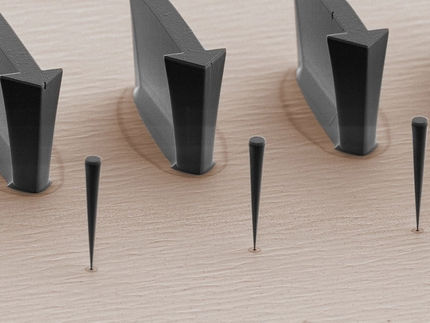
Over a period of about four hours, the wires grew to a length of some 4000 nanometres. One nanometre (nm) is one millionth of a millimetre. However, not only did the wires become longer during this time, but also thicker: their diameter increased from an initial 20 nm to up to 140 nm at the top of the wire, still making them around 500 times thinner than a human hair.
"One rather exciting feature is that the images taken under the electron microscope show the nanowires to have a slightly different shape," says co-author Thomas Keller from DESY NanoLab. Although the wires were thicker at the top than at the bottom, just as indicated by the X-ray data, the diameter measured under the electron microscope was larger in the lower region of the wire than what was observed using X-rays.
"We found out that the growth of the nanowires is not only due to the VLS mechanism but that a second component also contributes, which we were able to observe and quantify for the first time in this experiment. This additional sidewall growth lets the wires gain width," explains Schroth. Independently of VLS growth, the vapour deposited material also attaches itself directly to the side walls, particularly in the lower region of the nanowire. This additional contribution can be determined by comparing the X-ray measurements taken early on during the growth of the wire, with the electron microscope measurement after growth has ended.
Furthermore, the gallium droplets are constantly becoming larger as further gallium is added in the course of the growth process. Using growth models, the scientists were able to deduce the shape of the droplets, which had also been affected by the increasing droplet size. The effect of this is far-reaching: "As the droplet changes in size, the angle of contact between the droplet and the surface of the wires also changes. Under certain circumstances, the wire then suddenly continues growing with a different crystal structure," says Feigl. Whereas the fine nanowires initially crystallise in a hexagonal, so-called wurtzite structure, this behaviour changes after some time and the wires adopt a cubic zinc blende structure as they continue to grow. This change is important when it comes to applications, since the structure and shape of the nanowires have important consequences for the properties of the resulting material.
Such detailed findings not only lead to a better understanding of the growth process; they also provide approaches for customising future nanowires to have special properties for specific applications - for example to improve the efficiency of a solar cell or a laser.
Original publication
"Radial Growth of Self-Catalyzed GaAs Nanowires and the Evolution of the Liquid Ga-Droplet Studied by Time-Resolved in situ X‐ray Diffraction"; Philipp Schroth, Julian Jakob, Ludwig Feigl, Seyed Mohammad Mostafavi Kashani, Jonas Vogel, Jörg Strempfer, Thomas F. Keller, Ullrich Pietsch, and Tilo Baumbach; Nano Letters; 2018


Other news from the department science


