Black phosphorus-based van der Waals heterostructures for mid-infrared light-emission applications
Advertisement


MIR spectra have been widely used for thermal imaging, molecule characterizations, and communications. MIR light source is the key component of MIR technologies. Among them, MIR light-emitting diodes (LED) show advantages of narrow linewidth, low power consumption and portability. Since the rediscovery of thin-film BP in 2014, it has received much attention due to its unique properties, such as in-plane anisotropy, high carrier mobility, and tunable band gap, etc., making BP a promising material for applications in electronics and optoelectronics.
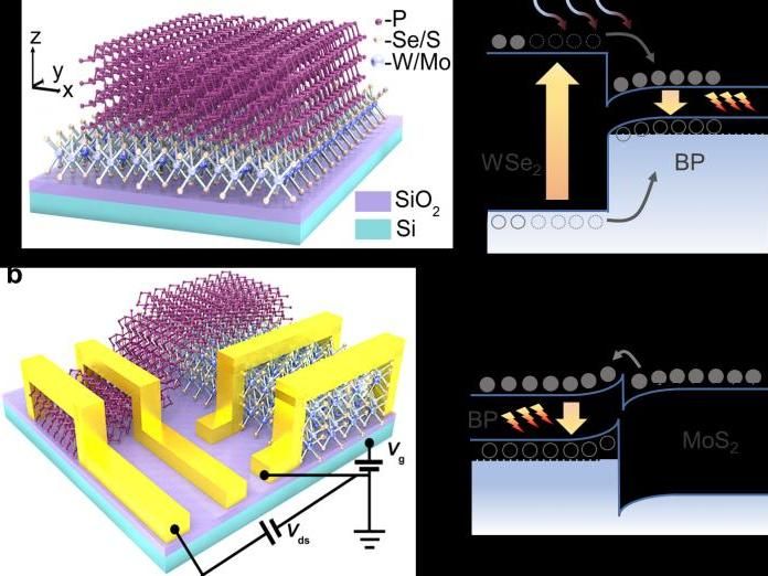
a, Schematic diagram of the BP-WSe2 heterostructure. Under the excitation of light, the electron and hole pairs in WSe2 can be efficiently transmitted to BP, thereby enhancing its MIR photoluminescence. b, Schematic diagram of the BP-MoS2 heterojunction diode. Under a positive bias voltage between BP and MoS2, the electrons on the conduction band of MoS2 can overcome the barrier, enter into the conduction band of BP, and recombine with abundant holes in BP. Thereby electroluminescence is achieved
Xinrong Zong, Huamin Hu, Gang Ouyang, Jingwei Wang, Run Shi, Le Zhang, Qingsheng Zeng, Chao Zhu, Shouheng Chen, Chun Cheng, Bing Wang, Han Zhang, Zheng Liu, Wei Huang, Taihong Wang, Lin Wang and Xiaolong Chen
BP has a thickness-dependent (0.3-2 eV) bandgap, and the bandgap size can be further tuned through introducing external electric field or chemical doping. Because of these reasons, thin-film BP has been regarded as a star MIR material. Previous research mainly focused on the luminescence properties of monolayer and few-layer BP flakes (with layer number < 5 layers). However, the latest reports indicate that thin-film BP (> 7 layers) shows remarkable photoluminescence properties in MIR region.
In this report, we proposed a novel vdW heterostructure for MIR light-emission applications, built from BP and TMDC (such as WSe2 and MoS2). According to the DFT calculation, the BP-WSe2 heterostructure forms a type-I band alignment. Hence, the electron and hole pairs in the monolayer WSe2 can be efficiently transported into the narrow-bandgap BP, thereby enhancing the MIR photoluminescence of thin-film BP. An enhancement factor ~200% was achieved in the 5nm-thick BP-WSe2 heterostructure.
On the other hand, the BP-MoS2 heterostructure forms a type-II band alignment. A natural PN junction is formed at the interface between p-type BP and n-type MoS2. When a positive voltage bias is applied between BP and MoS2 (Vds > 0), electrons in the conduction band of MoS2 can cross the barrier and enter into the conduction band of BP. At the same time, the majority of holes are blocked at the interface inside BP due to the large Schottky barrier of the valence band. As a result, an efficient MIR electroluminescence is achieved in the BP-MoS2 heterostructure.
The BP-TMDC vdW heterostructures show many merits, such as simple fabrication process, high efficiency, and good compatibility with silicon technology. Hence, it provides a promising platform for investigating silicon-2D hybrid optoelectronic systems.


Other news from the department science


