Hot off the Press
Universal ink for microcontact printing
Advertisement


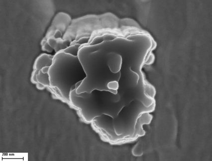
"Printing" on the micrometer scale is the technology of the future for the production of the electronic components used for such things as flat-screen monitors or (bio)sensors. Metal surfaces a few tens of square centimeters in size can already be structured without much experimental difficulty through a combination of microcontact printing and an etching process. Researchers are currently working to develop a simple production technology that is also broadly applicable for large surfaces. A team at Philips Research in Eindhoven in the Netherlands has now developed a universally applicable "ink" for microcontact printing.
The first step in microcontact printing is the production of an elastomeric malleable stamp by means of a mold. The stamp is then loaded with a special "ink" and is pressed onto the metal surface to be printed. The ink sticks to the metal surface and reproduces the microstructure of the stamp in a monomolecular layer. This monolayer acts as a corrosion-resistant mask in the subsequent etching process: the coated areas are not affected, whereas the metal in the uncoated areas is etched away, transferring the microstructure to the metal. Precious and coinage metals are both used, as are materials with oxidic surfaces, such as silicon and aluminum. Each type of surface requires a different type of ink to stick to it: precious and coinage metals need ink molecules that can be bound by means of a metal-sulfur bond. Oxidic surfaces bind molecules with an acid functionality, such as carboxylic acids or phosphonic acids. Substrates that have different types of metals on their surface are thus not easy to structure. Also, identical structures cannot be transferred onto different substrates with the same stamp, because once loaded, the stamp cannot be "washed" off and loaded with a different ink easily-and production of a new stamp is the most expensive part of the process.
The researchers led by Dirk Burdinski have now developed a universally applicable ink. It consists of a mixture of both types of ink, sulfur-containing octadecanethiol and octadecanephosphonic acid. When polydimethylsiloxane stamps are loaded with this ink, both types of metals can be structured. The individual components of the ink are selectively transferred to their corresponding surface without interfering with each other. This universal ink is potentially also useful for the coating of microfluidic systems on diagnostic chips, as these often have inner wall structures made of different materials. Also electronic component blocks requiring good adherence of the protective coating to different components could thus first be homogenized at the surface, allowing for better sealing.
Original publication. D. Burdinski et al.; "Universal Ink for Microcontact Printing"; Angewandte Chemie International Edition 2006.
Other news from the department science


These products might interest you
SprayMaster inspex by LaVision
Quality Control for Your Spraying Process Through Digital Spray and Particle Analysis
Reliable, Automated, Digital - The Geometry Measurement of Your Spraying Process in Real Time

FireSting-PRO by PyroScience
New fiber optic measuring device: Precise measurements even in the smallest volumes
Measure pH, oxygen and temperature even under sterile conditions

VEGAPULS | VEGABAR | VEGASWING by VEGA Grieshaber
Cyber-safe level measurement - here's how it works
Find out more about the unique sensor for liquid and solid media

Most read news


More news from our other portals


See the theme worlds for related content
Topic world Sensor technology
Sensor technology has revolutionized the chemical industry by providing accurate, timely and reliable data across a wide range of processes. From monitoring critical parameters in production lines to early detection of potential malfunctions or hazards, sensors are the silent sentinels that ensure quality, efficiency and safety.