New Materials for Making "Spintronic" Devices
Pushing the development of electronics beyond the limits of electric charge
An interdisciplinary group of scientists at the U.S. Department of Energy's Brookhaven National Laboratory has devised methods to make a new class of electronic devices based on a property of electrons known as "spin," rather than merely their electric charge. This approach, dubbed spintronics, could open the way to increasing dramatically the productivity of electronic devices operating at the nanoscale. The Brookhaven scientists have filed a U.S. provisional patent application for their invention, which is now available for licensing.
"This development can open the way for the use of spintronics in practical room temperature devices, an exciting prospect," said DOE Under Secretary for Science Raymond L. Orbach. "The interplay between outstanding facilities and laboratory researchers is a root cause for this achievement, and a direct consequence of the collaborative transformational research that takes place in our DOE laboratories."
In the field of electronics, devices based on manipulating electronic charges have been rapidly shrinking and, therefore, getting more efficient, ever since they were first developed in the middle of the last century. "But progress in miniaturization and increasing efficiency is approaching a fundamental technological limit imposed by the atomic structure of matter," said physicist Igor Zaliznyak, lead author on the Brookhaven Lab patent application. Once you've made circuits that approach the size of a few atoms or a single atom, you simply cannot make them any smaller.
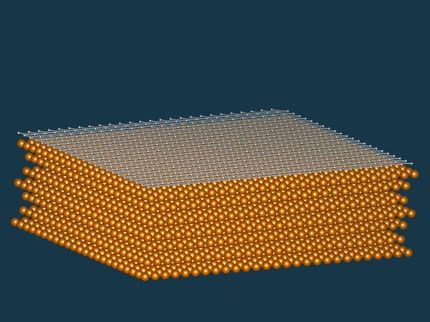
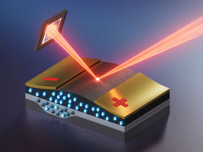
To move beyond this limit, Zaliznyak's team has been exploring ways to take advantage of an electron's "quantum spin" in addition to its electric charge. The Brookhaven group uses magnetism to manipulate spin in graphene, a material consisting of flat sheets of carbon atoms arranged in a hexagonal pattern. They've proposed ways to make materials consisting of layers of graphene mated to magnetic and nonmagnetic layers.
These "graphene-magnet multilayers" (GMMs) are expected to retain their properties at room temperature, an important practical requirement for spintronic devices. By properly arranging the magnetization of the magnetic layer(s), they can be used to create a full spectrum of spintronic devices, including (re-)writable microchips, transistors, logic gates, and more. Using magnetism for spin manipulation also opens exciting possibilities for creating active, re-writable and re-configurable devices whose function changes depending on the magnetization pattern written on the magnetic medium.
The patent application covers the methods for making the graphene-magnet multilayers, methods of using the GMMs, methods of magnetizing the GMMs, methods for measuring spintronic "current" in GMMs, and the spintronic devices made from GMMs.
Most read news
Other news from the department science

Get the chemical industry in your inbox
From now on, don't miss a thing: Our newsletter for the chemical industry, analytics, lab technology and process engineering brings you up to date every Tuesday and Thursday. The latest industry news, product highlights and innovations - compact and easy to understand in your inbox. Researched by us so you don't have to.
