NUS scientists use low cost technique to improve properties and functions of nanomaterials
Advertisement


NUS scientists use low cost technique to improve properties and functions of nanomaterials By 'drawing' micropatterns on nanomaterials using a focused laser beam, scientists could modify properties of nanomaterials for effective applications in photonic and optoelectric applications
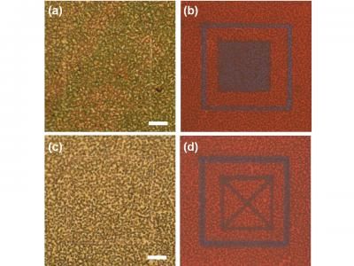
Mesoporous silicon nanowires were scanned by a focused laser beam in two different patterns, imaged by bright-field optical microscope, as depicted by (a) and (c), as well as fluorescence microscopy, as depicted by (b) and (d). Evidently, the images hidden in boxes shown in (a) and (c) are clearly revealed under fluorescence microscopy.
National University of Singapore
The challenges faced by researchers in modifying properties of nanomaterials for application in devices may be addressed by a simple technique, thanks to recent innovative studies conducted by scientists from the National University of Singapore (NUS).
Through the use of a simple, efficient and low cost technique involving a focused laser beam, two NUS research teams, led by Professor Sow Chorng Haur from the Department of Physics at the NUS Faculty of Science, demonstrated that the properties of two different types of materials can be controlled and modified, and consequently, their functionalities can be enhanced.
Said Prof Sow, "In our childhood, most of us are likely to have the experience of bringing a magnifying glass outdoors on a sunny day and tried to focus sunlight onto a piece of paper to burn the paper. Such a simple approach turns out to be a very versatile tool in research. Instead of focusing sunlight, we can focus laser beam onto a wide variety of nanomaterials and study effects of the focused laser beam has on these materials."
Micropatterns 'drawn' on MoS2 films could enhance electrical conductivity and photoconductivity
Molybdenum disulfide (MoS2), a class of transition metal dichalcogenide compound, has attracted great attention as an emerging two-dimensional (2D) material due to wide recognition of its potential in and optoelectronics. One of the many fascinating properties of 2D MoS2 film is that its properties depend on the thickness of the film. In addition, its properties can be modified once the film is modified chemically. Hence one of the challenges in this field is the ability to create microdevices out of the MoS2 film comprising components with different thickness or chemical nature.
To address this technological challenge, Prof Sow, Dr Lu Junpeng, a postdoctoral candidate from the Department of Physics at the NUS Faculty of Science, as well as their team members, utilised an optical microscope-focused laser beam setup to 'draw' micropatterns directly onto large area MoS2 films as well as to thin the films.
With this simple and low cost approach, the scientists were able to use the focused laser beam to selectively 'draw' patterns onto any region of the film to modify properties of the desired area, unlike other current methods where the entire film is modified.
Interestingly, they also found that the electrical conductivity and photoconductivity of the modified material had increased by more than 10 times and about five times respectively. The research team fabricated a photodetector using laser modified MoS2 film and demonstrated the superior performance of MoS2 for such application.
Other news from the department science