Tunable semiconductors possible with hot new material called graphene
Advertisement


Today's transistors and light emitting diodes (LED) are based on silicon and gallium arsenide semiconductors, which have fixed electronic and optical properties. Now, University of California, Berkeley, researchers have shown that a form of carbon called graphene has an electronic structure that can be controlled by an electrical field, an effect that can be exploited to make tunable electronic and photonic devices.
While such properties were predicted for a double layer of graphene, this is the first demonstration that bilayer graphene exhibits an electric field-induced, broadly tunable bandgap, according to principal author Feng Wang, UC Berkeley assistant professor of physics. The bandgap of a material is the energy difference between electrons residing in the two most important states of a material - valence band states and conduction band states - and it determines the electrical and optical properties of the material.
"The real breakthrough in materials science is that for the first time you can use an electric field to close the bandgap and open the bandgap. No other material can do this, only bilayer graphene," Wang said.
Because tuning the bandgap of bilayer graphene can turn it from a metal into a semiconductor, a single millimeter-square sheet of bilayer graphene could potentially hold millions of differently tuned electronic devices that can be reconfigured at will, he said.
Wang, post-doctoral fellow Yuanbo Zhang, graduate student Tsung-Ta Tang and their UC Berkeley and Lawrence Berkeley National Laboratory (LBNL) colleagues report their success in Nature .
"The fundamental difference between a metal and a semiconductor is this bandgap, which allows us to create semiconducting devices," said coauthor Michael Crommie, UC Berkeley professor of physics. "The ability to simply put a material between two electrodes, apply an electric field and change the bandgap is a huge deal and a major advance in condensed matter physics, because it means that in a device configuration we can change the bandgap on the fly by sending an electrical signal to the material."
While a single layer of graphene has a zero bandgap, two layers of graphene together theoretically should have a variable bandgap controlled by an electrical field, Wang said. Previous experiments on bilayer graphene, however, have failed to demonstrate the predicted bandgap structure, possibly because of impurities. Researchers obtain graphene with a very low-tech method: They take graphite, like that in pencil lead, smear it over a surface, cover with Scotch tape and rip it off. The tape shears the graphite, which is just billions of layers of graphene, to produce single- as well as multi-layered graphene.
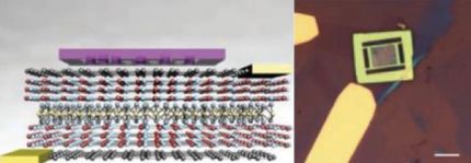
Wang, Zhang, Tang and their colleagues decided to construct bilayer graphene with two voltage gates instead of one. When the gate electrodes were attached to the top and bottom of the bilayer and electrical connections (a source and drain) made at the edges of the bilayer sheets, the researchers were able to open up and tune a bandgap merely by varying the gating voltages. The team also showed that it can change another critical property of graphene, its Fermi energy, that is, the maximum energy of occupied electron states, which controls the electron density in the material.
"With top and bottom gates on bilayer graphene, you can independently control the two most important parameters in a semiconductor: You can change the electronic structure to vary the bandgap continuously, and independently control electron doping by varying the Fermi level," Wang said.
Because of charge impurities and defects in current devices, the graphene's electronic properties do not reflect the intrinsic graphene properties. Instead, the researchers took advantage of the optical properties of bandgap materials: If you shine light of just the right color on the material, valence electrons will absorb the light and jump over the bandgap.
In the case of graphene, the maximum bandgap the researchers could produce was 250 milli-electron volts (meV). (In comparison, the semiconductors germanium and silicon have about 740 and 1,200 meV bandgaps, respectively.) Putting the bilayer graphene in a high intensity infrared beam produced by LBNL's Advanced Light Source (ALS), the researchers saw absorption at the predicted bandgap energies, confirming its tunability. Because the zero to 250 meV bandgap range allows graphene to be tuned continuously from a metal to a semiconductor, the researchers foresee turning a single sheet of bilayer graphene into a dynamic integrated electronic device with millions of gates deposited on the top and bottom.
"All you need is just a bunch of gates at all positions, and you can change any location to be either a metal or a semiconductor, that is, either a lead to conduct electrons or a transistor," Zhang said. "So basically, you don't fabricate any circuit to begin with, and then by applying gate voltages, you can achieve any circuit you want. This gives you extreme flexibility."


Other news from the department science


