Social Distancing on the Nanoscale
New contact-free nanoscopy concept
Advertisement


A team of physicists from Germany, the US and the UK managed to observe the motion of electrons from one atomically thin layer into an adjacent one with nanoscale spatial resolution. The new contact-free nanoscopy concept, which shows great potential for investigations into conducting, nonconducting and superconducting materials, will be introduced in the new volume of the science journal Nature Photonics.
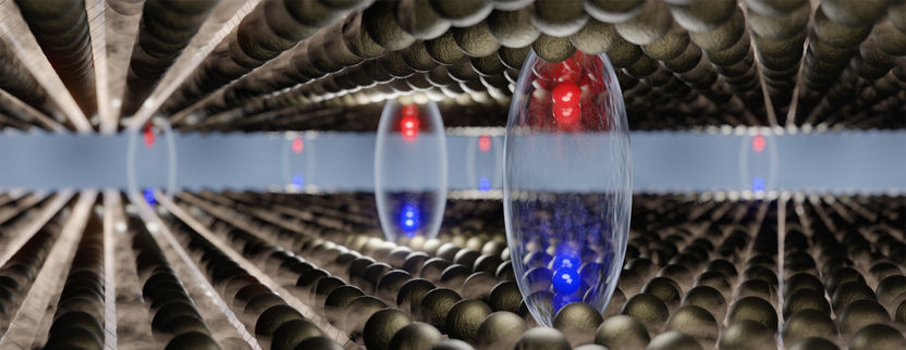
Interlayer excitons (glossy ellipsoids), which can form after electrons and holes (red and blue spheres) are separated between optically excited, atomically thin layers (top and bottom sheet).
©Markus Plankl (2021)
Nanotechnology sometimes still sounds like science fiction, but is already an integral part of modern electronics in our computers, smart phones or cars. The size of electronic components, like transistors or diodes has reached the nanoscale, corresponding to only one millionth of a millimeter. This makes conventional optical microscopes no longer sufficient for inspecting these nanostructures. To develop innovative future nanotechnology, scientists have replaced the optical microscope with much more sophisticated concepts, such as electron or scanning tunneling microscopy. However, these techniques use electrons instead of light, which can influence the properties of the nanoscale devices. Furthermore, these important measurement techniques are limited to electrically conducting samples.
A team of physicists around Rupert Huber and Jaroslav Fabian at the Regensburg Center for Ultrafast Nanoscopy (RUN) at Universität Regensburg together with colleagues Tyler Cocker from Michigan State University, USA, and Jessica Boland from the University of Manchester, UK, have introduced a new technique, which can resolve electron motion on the nanoscale without needing to be electrically contacted. Better still, the new method also reaches unbelievable time resolution as good as one quadrillionth of a second (the femtosecond timescale). Combining these extreme spatial and temporal resolutions makes the recording of slow-motion movies of ultrafast electron dynamics on the nanoscale possible.
The concept behind the technique works similar to contactless payment (Chipcard, Phone, Scanner), which has become an increasingly common component in our lives since the start of the pandemic. These payment methods are based on established frequencies and protocols on the macroscale such as Near Field Communication (NFC). Here, the scientists transferred this idea down to the nanoscale by using a sharp metallic tip as a nano-antenna, which is brought close to the investigated sample. In contrast to the aforementioned established techniques, where tips are used to drive a current through the sample, the new concept uses a weak alternating electric field to scan the sample contactlessly. The frequency used in the experiments is boosted to the terahertz spectral range, approximately 100,000 times higher than the one used in NFC scanners. Minute changes in these weak electric fields allow for precise conclusions about the local electron motion within the material. Combining the measurements with a realistic quantum theory shows that the concept even allows for quantitative results. In order to achieve high temporal resolution additionally, the physicists used extremely short light pulses to record crisp snapshots of the movement of electrons over nanometer distances.
The team chose a sample of a new material class called transition metal dichalcogenides, which can be produced in atomically thin layers, as their first test sample. When these sheets are stacked under freely chosen angles, new artificial solids emerge with novel material properties, which are prominently investigated in the Collaborative Research Center 1277 in Regensburg. The sample under study was made from two different atomically thin dichalcogenides to test the centerpiece of a futuristic solar cell. When shining green light onto the structure, charge carriers emerge that will move in one or the other direction depending on their polarity – the basic principle of a solar cell, which converts light into electricity. The ultrafast charge separation was observed by the scientists in time as well as in space with nanometer precision. To their surprise, the charge separation even works reliably when the dichalcogenide layers lay over tiny impurities like a mini carpet – important insights to optimize these new materials for the future use in solar cells or computer chips.
The researchers are exhilarated by their insightful results. “We can’t wait to videotape further fascinating charge transfer processes in insulating, conducting and superconducting materials.”, explains Markus Plankl, first author of the publication. Postdoctoral colleague and co-author Thomas Siday adds: ”Insights on the ultrafast transport on the relevant length and timescales will help us to understand how tunneling shapes the functionalities in a wide range of condensed matter systems.” Besides nanostructures in physics, previously elusive quantum processes in biological systems can now be accessed. These results reflect the increasing focus of researchers from biology, chemistry and physics at the University of Regensburg towards ultrafast nanoscopy, which led to the approval of the new Regensburg Center for Ultrafast Nanoscopy (RUN). The RUN building, which is currently under construction on the University campus, should provide the optimal environment for such an interdisciplinary exploration of the nanocosm.
Original publication
M. Plankl, P. E. Faria Junior, F. Mooshammer, T. Siday, M. Zizlsperger, F. Sandner, F. Schiegl, S. Maier, M. A. Huber, M. Gmitra, J. Fabian, J. L. Boland, T. L. Cocker and R. Huber; "Subcycle contact-free nanoscopy of ultrafast interlayer transport in atomically thin heterostructures"; Nature Photonics; 2021


Other news from the department science


