How to keep data safe on the long run
Team presents new path to long-term data storage based on atomic-scale defects
Advertisement


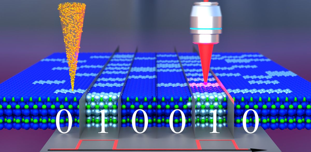
With the development of the internet, social media or cloud computing, the amount of data created worldwide on a daily basis is sky-rocketing. This calls for new technologies which could provide higher storage densities combined with secure long-term data archiving far beyond the capabilities of traditional data storage devices. An international research team led by the Helmholtz-Zentrum Dresden-Rossendorf (HZDR) now proposes a new concept of long-term data storage based on atomic-scale defects in silicon carbide, a semiconducting material. These defects are created by a focused ion beam, providing high spatial resolution, fast writing speed and low energy for storing a single bit, as the team reports in the journal Advanced Functional Materials.
Latest estimates assume around 330 million terabytes of new data created each day, with 90 percent of the world's data generated in the last two years alone. If the sheer numbers already suggest the need of advanced data storage technologies, it is by no means the only problem associated to this development. “The limited storage time of current storage media requires data migration within several years to avoid any data loss. Besides of being trapped in perpetual data migration procedures, this substantially increases the energy consumption, because a significant amount of energy is consumed in the process”, says Dr. Georgy Astakhov from the Institute of Ion Beam Physics and Materials Research at HZDR.
To mitigate this looming crisis, Astakhov's team now introduces a new concept of long-term data storage based on atomic-scale defects in silicon carbide. These defects are inflicted by a focused beam of protons or helium ions and read using luminescence mechanisms associated to the defects.
Traditional storage devices throttled by physics
Currently, magnetic memory is the prime choice when it comes to data storage solutions aiming for large capacities, while the laws of physics set the limits to achievable storage densities. To increase them, the size of the magnetic particles must shrink. But then, thermal fluctuations and diffusion processes in the material gain in importance, with deteriorating impact on storage time. Tuning magnetic properties of the material might suppress this effect, but this comes with a price tag: a higher energy to store information. Similarly, the performance of optical devices is thwarted by the laws of physics as well. Due to the so-called diffraction limit, the smallest recording bit is restricted in size: It cannot get any smaller than half of the light wavelength, setting the limit of the maximum storage capacity. The way out is multi-dimensional optical recording.
Silicone carbide features atomic-scale defects, especially the absence of silicon atoms in the lattice site. The defects are created by a focused proton or helium ion beam, providing high spatial resolution, fast writing speed and low energy for storing a single bit. “The diffraction limit of storage density inherent to optical media applies as well in our case. We overcome it by 4D encoding schemes. Here, the three spatial dimensions and an additional fourth intensity dimension are realized by controlling the lateral position and depth as well as the number of defects. Then we optically read out the stored data by means of photoluminescence provoked by optical excitation. Furthermore, the areal storage density can be significantly improved using focused electron-beam excitation causing observable cathodoluminescence”, Astakhov highlights some prominent features of his method.
Storing data for generations
The stored information could be knocked-out of the defects again, depending on environmental conditions in which the medium is kept, but the scientists have good news considering their material: “The temperature-dependent deactivation of these defects suggests a retention time minimum over a few generations under ambient conditions”, says Astakhov. And there is more. With near-infrared laser excitation, modern encoding techniques and multi-layer data storage, namely the stacking of up to ten silicon carbide layers on top of each other, the team reaches an areal storage density which corresponds to that of Blu-ray discs. Switching to electron-beam excitation instead of optical excitation for the data read-out, the limit achievable in this manner corresponds to a currently reported record areal storage density of a prototype magnetic tape, which has, however, shorter storage time and higher energy consumption.
For this work, the Rossendorf scientists joined forces with researchers from Julius-Maximilian University Würzburg (Germany), Jet Propulsion Laboratory, California Institute of Technology (USA), National Institutes for Quantum Science and Technology (Japan), and Tohoku University (Japan). The team's conceptual approach is not limited to silicon carbide and can be extended to other materials with optically active defects, including 2D materials.
Original publication


Other news from the department science


