Turning down the noise in graphene
graphene is a two-dimensional crystalline sheet of carbon atoms - meaning it is only one atom thick - through which electrons can race at nearly the speed of light - 100 times faster than they can move through silicon. This plus graphene's incredible flexibility and mechanical strength make the material a potential superstar for the electronics industry. However, whereas the best electronic materials feature a strong signal and weak background noise, attaining this high signal-to-noise ratio has been a challenge for both single and bi-layers of graphene, especially when placed on a substrate of silica or some other dielectric. One of the problems facing device developers has been the lack of a good graphene noise model.
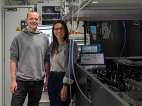
Working with the unique nanoscience capabilities of the Molecular Foundry at the U.S. Department of Energy (DOE)'s Lawrence Berkeley National Laboratory, a multi-institutional team of researchers has developed the first model of signal-to-noise-ratios for low frequency noises in graphene on silica. Their results show noise patterns that run just the opposite of noise patterns in other electronic materials.
Berkeley Lab materials scientist Yuegang Zhang led a study in which it was determined that for graphene on silica, the background signal noise is minimal near the region in the graphene where the electron density of states (the number of energy states available to each electron) is lowest. For semiconductors, such as silicon, in the region where electron density states is low the background noise is at its highest. However, there were distinct differences in the noise patterns of single and bi-layer graphene.
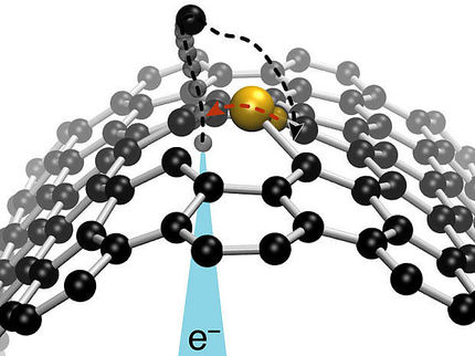
"In this work, we present the four-probe low frequency noise characteristics in single- and bi-layer graphene samples, using a back-gated device structure that helps simplify the physics in understanding the interactions between the graphene and the silica substrate," says Zhang. "For single-layer graphene we found that the noise was reduced either close to or far away from the lowest electron density of states, sometimes referred to as the Dirac point for graphene, forming an M-shaped pattern. For the bi-layer graphene, we found a similar noise reduction near the Dirac point but an increase away from that point, forming a V-shaped pattern. The noise data near the Dirac point correlated to spatial-charge inhomogeneity."
Lead author Guangyu Xu, a physicist with the Department of Electrical Engineering at the University of California (UC) Los Angeles, says the spatial charge inhomogeneity responsible for the graphene's unique noise patterns was probably caused by the charge impurities near the graphene-substrate interface.
"Our experiment carefully rules out other possible extrinsic factors that might influence the result," Xu says. "We conclude the correlation between the anomalous noise feature and the spatial charge inhomogeneity, is one of the main carrier scattering mechanisms for unsuspended graphene samples."
Xu says this model of low frequency noise characteristics in graphene should be a significant help for fabricating electronic devices because biasing at the low noise regime can be designed into the device.
"This will benefit the high signal-to-noise ratio in graphene," Xu says.
Original publication: "Effect of Spatial Charge Inhomogeneity on 1/f Noise Behavior in Graphene"; Nano Letters
Other news from the department science


Get the chemical industry in your inbox
From now on, don't miss a thing: Our newsletter for the chemical industry, analytics, lab technology and process engineering brings you up to date every Tuesday and Thursday. The latest industry news, product highlights and innovations - compact and easy to understand in your inbox. Researched by us so you don't have to.