Researchers discover new phase of boron nitride and a new way to create pure c-BN
Advertisement


Researchers at North Carolina State University have discovered a new phase of the material boron nitride (Q-BN), which has potential applications for both manufacturing tools and electronic displays. The researchers have also developed a new technique for creating cubic boron nitride (c-BN) at ambient temperatures and air pressure, which has a suite of applications, including the development of advanced power grid technologies.
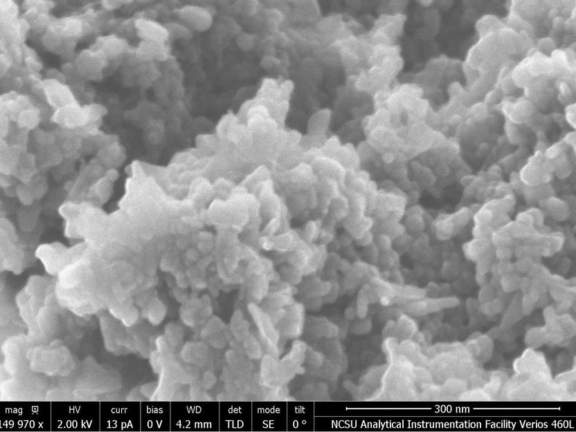
This image shows cubic boron nitride nanocrystallites.
Anagh Bhaumik
"This is a sequel to our Q-carbon discovery and converting Q-carbon into diamond," says Jay Narayan, the John C. Fan Distinguished Chair Professor of Materials Science and Engineering at NC State and lead author of a paper describing the research. "We have bypassed what were thought to be the limits of boron nitride's thermodynamics with the help of kinetics and time control to create this new phase of boron nitride.
"We have also developed a faster, less expensive way to create c-BN, making the material more viable for applications such as high-power electronics, transistors and solid state devices," Narayan says. "C-BN nanoneedles and microneedles, which can be made using our technique, also have potential for use in biomedical devices." C-BN is a form of boron nitride that has a cubic crystalline structure, analogous to diamond.
Early tests indicate that Q-BN is harder than diamond, and it holds an advantage over diamond when it comes to creating cutting tools. Diamond, like all carbon, reacts with iron and ferrous materials. Q-BN does not. The Q-BN has an amorphous structure, and it can easily be used to coat cutting tools, preventing them from reacting with ferrous materials.
"We have also created diamond/c-BN crystalline composites for next-generation high-speed machining and deep-sea drilling applications," Narayan says. "Specifically, we have grown diamond on c-BN by using pulsed laser deposition of carbon at 500 degrees Celsius without the presence of hydrogen, creating c-BN and diamond epitaxial composites."
The Q-BN also has a low work function and negative electron affinity, which effectively means that it glows in the dark when exposed to very low levels of electrical fields. These characteristics are what make it a promising material for energy-efficient display technologies.
To make Q-BN, researchers begin with a layer of thermodynamically stable hexagonal boron nitride (h-BN), which can be up to 500-1000 nanometers thick. The material is placed on a substrate and researchers then use high-power laser pulses to rapidly heat the h-BN to 2,800 degrees Kelvin, or 4,580 degrees Fahrenheit. The material is then quenched, using a substrate that quickly absorbs the heat. The whole process takes approximately one-fifth of a microsecond and is done at ambient air pressure.
By manipulating the seeding substrate beneath the material and the time it takes to cool the material, researchers can control whether the h-BN is converted to Q-BN or c-BN. These same variables can be used to determine whether the c-BN forms into microneedles, nanoneedles, nanodots, microcrystals or a film.
"Using this technique, we are able to create up to a 100- to 200-square-inch film of Q-BN or c-BN in one second," Narayan says.
By comparison, previous techniques for creating c-BN required heating hexagonal boron nitride to 3,500 degrees Kelvin (5,840 degrees Fahrenheit) and applying 95,000 atmospheres of pressure.
C-BN has similar properties to diamond, but has several advantages over diamond: c-BN has a higher bandgap, which is attractive for use in high-power devices; c-BN can be "doped" to give it positively- and negatively-charged layers, which means it could be used to make transistors; and it forms a stable oxide layer on its surface when exposed to oxygen, making it stable at high temperatures. This last characteristic means it could be used to make solid state devices and protective coatings for high-speed machining tools used in oxygen-ambient environments.
"We're optimistic that our discovery will be used to develop c-BN-based transistors and high-powered devices to replace bulky transformers and help create the next generation of the power grid," Narayan says.
Original publication


Other news from the department science


