Nitrades in transition
Advertisement


The average, everyday person might not be familiar with gallium nitride, also known as GaN, but there is a good chance they've heard of silicon, a semiconductor that's been used for decades and found in every computer and most electronics.
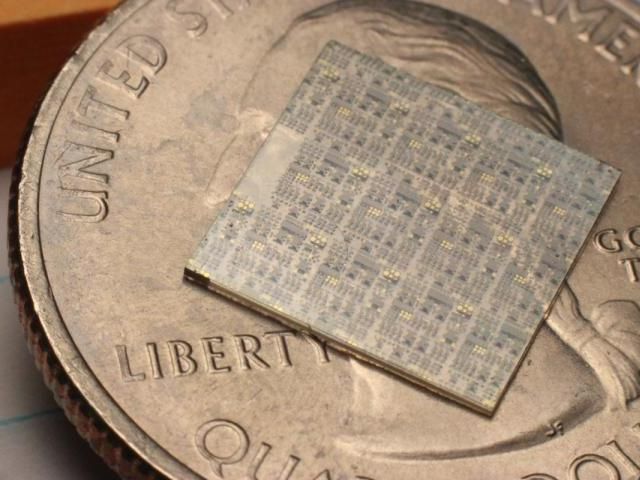
US Naval Research Laboratory (NRL) researchers have developed a patent pending technique using niobium nitride (Nb2N) that allows Gallium Nitride (GaN) to be transferred onto almost anything.
U.S. Naval Research Laboratory
As a semiconductor, GaN is similar to silicon, but it differs in its elemental makeup and properties, which makes it a more robust, rugged type of electronic material. GaN's qualities allow it to operate at nearly five times higher power and temperature than silicon and commercial commodity semiconductors in certain applications.
Solid-state (or LED) lighting and wireless data transmitters for cell phone base stations are two examples where GaN has made a considerable impact over the past few years. Power switching components for solar inverters and electric vehicles are also moving towards GaN technology due to its ability to improve efficiency.
"GaN technology ultimately saves energy compared to incumbent technologies and can typically be packaged in smaller and lighter form factors," said Dr. David Meyer, U.S. Naval Research Laboratory (NRL) section head for wide bandgap materials and devices in the Electronics Science and Technology Division.
During the 90s, the Navy and other DoD agencies invested a large amount of funding in basic research of GaN technology for RF wireless technology. Over the past few years it has successfully graduated from the research lab and is now used in military systems such as the Air and Missile Defense Radar (AMDR) and Next Generation Jammer.
Meyer's group at NRL has continued to push nitride materials research forward and recently made an important breakthrough in the ability to grow thin films of a transition metal nitride called niobium nitride (Nb2N). The thin crystalline material has a similar structure to GaN; however, its electrical and physical properties are dramatically different. For instance, Nb2N is metallic instead of semiconducting and can become superconductive at cryogenic temperatures.
"We have determined that Nb2N has several unique properties that can lead to the realization of new microelectronic devices and circuits," said Meyer.
One property of the new material is how it dissolves away in a reactive gas, while leaving nearby GaN electronics untouched. By inserting a thin layer of Nb2N between a GaN transistor, LED, or circuit and the substrate the material is grown on, Meyer and his team can perform a patent-pending lift-off technique, which allows it to be transferred onto nearly anything.
"We have this method and it's really flexible. We anticipate that there are several applications that would benefit from having GaN technology integrated at the device or circuit level," said Meyer.


Other news from the department science


