Gold nanoantennas help in creation of more powerful nanoelectronics
Advertisement


Scientists from Tomsk Polytechnic University and their colleagues from Germany have conducted an experiment which demonstrated the behavior of areas of two-dimensional materials which are applied in advanced electronics. It comes to devices that are in the research stage and will be used for the creation of flexible displays for smartphones and other gadgets, flexible optical and computing schemes, flexible solar cells and so on. According to the authors of the study, these are the experiments that have not been conducted before. The scientists are working on a technology which allows us to see how materials interact at the nanoscale, to determine local strain occurring at their interaction and even to see defects of the materials at the nanoscale that will make it possible to improve the components of nanoelectronics.
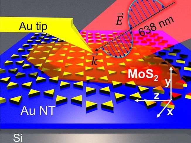
This is a schematic of the experiment.
Tomsk Polytechnic University
'Now in the field of electronics and digital technology there is a trend to miniaturize the devices. This trend is most relevant for transistors,' - says Prof. Raul Rodrigez from the Department of Lasers and Lighting Technology. - 'Nowadays there are modern technologies which enable the creation of transistors with a channel width of 12 to 14 nanometers, thus placing more transistors in the processor, increasing the productivity of smartphones and other miniature electronic devices. To further improve these technologies and create transistors of even smaller sizes, we should understand how the semiconductor material behaves when interacting with metals and how its properties change at the nanoscale.'
Earlier, according to the scientists, component materials of modern electronics were studied only at the macro- and micro-scale, but data obtained was not always sufficient to understand the interaction of materials with each other. In the published paper the scientists from TPU and Chemnitz Technological University and the University of Regensburg (Germany) demonstrated for the first time how component materials of advanced nanoelectronics behave at the nanoscale.
'For the creation of the complete line of different devices used in nanoelectronics, in particular flexible ones, various classes of two-dimensional materials are required, including semiconductors. Molybdenum disulfide is one of the most famous semi-conductors. Our goal was to study strain occurring in this material at the nanoscale, as well as the processes of its stretching or compressing in different structures and fields,' - say the authors of the research paper.
The scientists used gold nanoparticles, i.e. nanotriangles. Two monolayers of molybdenum disulphide were placed on top of them, which was transformed due the convex shape of the nanotriangles, what caused local strain 1.4%.
'The strain is more than we initially expected to see. In general, we had no goal to create the highest possible strain, but it's interesting that simply putting thin layers of molybdenum disulfide on metal we may obtain such significant deformations. This is very important to understand what happens when a semiconductor (molybdenum disulfide) contacts a conductor (gold) if we want to create a nanodevice,' notes Prof. Rodrigez. - 'In our work we shown that we can't neglect the interaction between a thin film and a substrate in electron nanodevices. When these materials are studied, all their properties are investigated on a flat substrate. However, a metal used in electrodes may change the properties of the material. This is inevitable, but perhaps it can be used in a way.'
Raul Rodrigez specifies that the published article was the first one describing such local measurements of strain.
The experiment was a success due to a unique technology Tip-Enhanced Raman Spectroscopy (TERS) combining methods of optical spectroscopy and atomic force microscopy. The main element of the technology is a gold nano-antenna embedded in the atomic-force microscope. It size varies from microns at the base to nanometers at the tip. A nanoparticle is placed on the tip of the antenna and scientists study only signals received from this nanoparticle.
The scientists emphasize that the TERS method is applicable both for studying local strain and interaction processes of particles and detecting defects in certain materials at the nanoscale.
Original publication


Other news from the department science


Most read news


More news from our other portals


See the theme worlds for related content
Topic World Spectroscopy
Investigation with spectroscopy gives us unique insights into the composition and structure of materials. From UV-Vis spectroscopy to infrared and Raman spectroscopy to fluorescence and atomic absorption spectroscopy, spectroscopy offers us a wide range of analytical techniques to precisely characterize substances. Immerse yourself in the fascinating world of spectroscopy!