One transistor for all purposes
Organic semiconductors
Advertisement


In mobiles, fridges, planes – transistors are everywhere. But they often operate only within a restricted current range. LMU physicists have now developed an organic transistor that functions perfectly under both low and high currents.
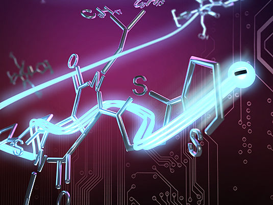
Christoph Hohmann, Nanosystems Initiative Munich (NIM)
Transistors are semiconductor devices that control voltage and currents in electrical circuits. To reduce economic and environmental costs, electronic devices must become smaller and more effective. This applies above all to transistors. In the field of inorganic semiconductors, dimensions below 100 nanometers are already standard. In this respect, organic semiconductors have not been able to keep up. In addition, their performance with regard to charge-carrier transport is considerably worse. But organic structures offer other advantages. They can easily be printed on an industrial scale, the material costs are lower, and they can be transparently applied to flexible surfaces.
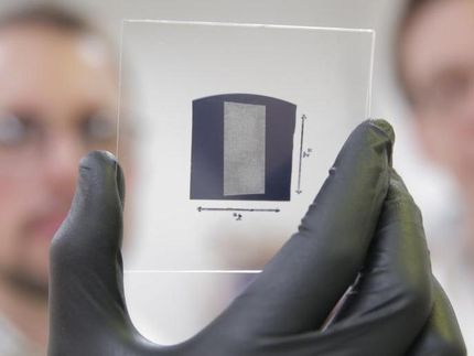
Thomas Weitz, a professor in LMU’s Faculty of Physics and a member of the Nanosystems Initiative Munich, and his team are working intensively on the optimization of organic transistors. In their latest publication in Nature Nanotechnology, they describe the fabrication of transistors with an unusual structure, which are tiny, powerful and above all versatile. By carefully tailoring a small set of parameters during the production process, they have been able to design nanoscale devices for high or low current densities. The primary innovation lies in the use of an atypical geometry, which also facilitates assembly of the nanoscopic transistors.
“Our aim was to develop a transistor design which combines the ability to drive high currents that is typical of classical transistors with the low-voltage operation required for use as artificial synapses,” says Weitz. With the successful assembly and characterization of vertical organic field-effect transistors with exactly selectable dimensions and an ionic gating, this goal has now been achieved.
Potential areas of application for the new devices include OLEDs and sensors where low voltages, high ON-state current densities or large transconductances are required. Of special interest is their possible use in so-called memristive elements. “Memristors can be thought of as artificial neurons, as they can be used to model the behavior of neurons when processing electrical signals,” explains Weitz. “By fine-tuning the geometry of a memristive device, it could be applied in a variety of contexts, such as learning processes in artificial synapses.” The researchers have already submitted a patent application for the device to enable them to develop the new transistor architecture for industrial use.
Original publication


Other news from the department science


