Surprisingly strong and deformable silicon
The strength of lithographically produced silicon pillars even reached values that one would only expect only in theory
Advertisement


Researchers at ETH and Empa have shown that tiny objects can be made from silicon that are much more deformable and stronger than previously thought. In this way, sensors in smartphones could be made smaller and more robust.
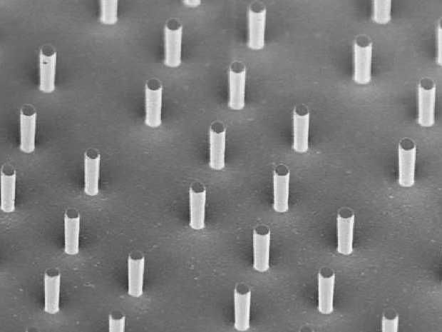
A few micrometer silicon columns under the electron microscope: Such structures make the material more elastic.
Laszlo Pethö / Empa
Since the invention of the MOSFET transistor sixty year ago, the chemical element silicon on which it is based has become an integral part of modern life. It ushered in the computer age, and by now the MOSFET has become the most produced device in history. Silicon is readily available, cheap, and has ideal electrical properties, but also one important drawback: it is very brittle and, therefore, breaks easily. This can become a problem when trying to make micro-electro-mechanical systems (MEMS) from silicon, such as the acceleration sensors in modern smartphones.
At ETH in Zurich, a team led by Jeff Wheeler, Senior Scientist at the Laboratory for Nanometallurgy, together with colleagues at the Laboratory for Mechanics of Materials and Nanostructures at Empa, has shown that, under certain conditions, silicon can be much stronger and more deformable than was previously thought.
Ten-year effort
“This is the result of a ten-year effort”, says Wheeler, who worked as a researcher at Empa prior to his career at ETH. To understand how tiny silicon structures can deform, within the framework of an SNF project, he took a closer look at a widely used production method: the focused ion beam. Such a beam of charged particles can mill desired shapes into a silicon wafer very effectively, but in doing so leaves behind distinct traces in the form of surface damage and defects, which cause the material to break more easily.
Lithography with final cleaning
Wheeler and his collaborators had the idea to try a particular type of lithography as an alternative to the ion beam method. “First, we produce the desired structures – tiny pillars in our case – by etching away un-masked material from the areas of the silicon surface using a gas plasma”, explains Ming Chen, a former PhD student in Wheeler’s group. In a further step, the surface of the pillars, some of which are narrower than a hundred nanometres, are first oxidized and then cleaned by completely removing the oxide layer with a strong acid.
Chen then studied the strength and plastic deformability of silicon pillars of different widths with an electron microscope and compared the two production methods. To that end, he pressed a tiny diamond punch into the pillars and studied their deformation behaviour in the electron microscope.
Striking results
The results were striking: the pillars that had been milled with an ion beam collapsed at a width of less than half a micrometre. By contrast, the pillars produced by lithography only suffered brittle fractures at widths above four micrometres, while thinner pillars were able to withstand the strain much better. “These lithographic silicon pillars can deform at sizes ten times greater than what we’ve seen in ion beam-machined silicon with the same crystal orientation, with double the strength!”, Wheeler summarizes the results of his experiments.
The strength of the lithographically produced pillars even reached values that one would only expect only in theory, for ideal crystals. What makes the difference here, says Wheeler, is the absolute purity of the surfaces of the pillars, which is achieved by the final cleaning step. This results in a much smaller number of surface defects from which a fracture could originate. With the assistance of Alla Sologubenko, a researcher with the microscopy centre ScopeM at ETH, this additional deformability also allowed the team to observe a striking change in deformation mechanisms at smaller sizes. This revealed new details on how silicon can deform.
Applications in smartphones
The results obtained by ETH researchers could have an immediate impact on the fabrication of silicon MEMS, Wheeler says: “In this way, the gyroscopes used in smartphones, which detect rotations of the device, could be made even smaller and more robust.” That shouldn’t be too difficult to realize, given that industry is already using the combination of etching and cleaning Wheeler and his colleagues investigated. The method could also be applied to other materials having crystal structures similar to that of silicon, the researchers believe. Moreover, more elastic silicon could also be used to further improve the electrical properties of the material for certain applications. By applying a large strain of the semiconductor the mobility of its electrons can be increased, which can lead, for instance, to shorter switching times. So far, one had to produce nanowires to achieve that, but now this could be done directly using structures integrated into a semiconductor chip.
Original publication


Other news from the department science


