Producing defectless metal crystals of unprecedented size
A new method to obtain large single crystals up to 32 square centimeters
Advertisement
A research group at the Center for Multidimensional Carbon Materials, within the Institute for Basic Science (IBS), have published a new method to convert inexpensive polycrystalline metal foils to single crystals with superior properties. It is expected that these materials will find many uses in science and technology.

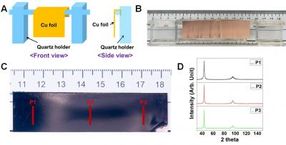
(A) Schematic of the quartz holder that the copper (Cu) foil is suspended from, (B) photograph of the configuration shown schematically in (A). (C) Photograph of the annealed single crystal Cu foil (about 2 cm × 8 cm), next to a ruler. (D) X-ray diffraction (XRD) spectra of the three regions in the annealed single crystal Cu foil indicated by P1-P3 in (C).
IBS
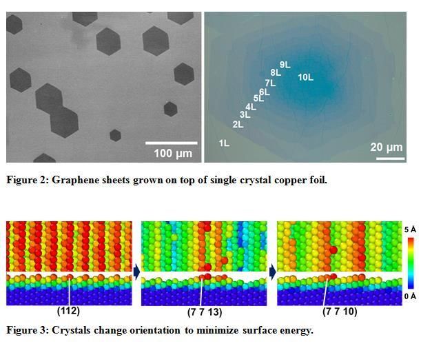
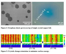
Figure 2: Graphene sheets grown on top of single crystal copper foil. (Left) Very high quality single crystal monolayer graphene was obtained on single crystal copper foil, and (right) multilayer graphene (from 2 to 10 layers) on a single crystal copper-nickel alloy foil.Figure 3: Crystals change orientation to minimize surface energy. Members of the team, DING Feng, ZHANG Leining, and DONG Jichen, contributed a model and theoretical calculations on 'colossal grain growth' that was observed and studied through experiments. SHIN Hyung-Joon drew attention to the importance of the initial "texture" of the polycrystalline metal foils and the role this plays in colossal grain growth. In the presence of large amounts of vacancies within the crystal structure (5 percent in these molecular dynamics simulation), the crystal orientation changes to minimize the surface energy.
IBS
The structure of most metal materials can be thought of as a patchwork of different tiny crystals, bearing some defects on the borders between each patch. These defects, known as grain boundaries (GBs), worsen the electrical and sometimes mechanical properties of the metal. Single crystal metals, instead, have no GBs and show higher electrical conductivity and other enhanced qualities that can play a major role in multiple fields, such as electronics, plasmonics, and catalysis, among others. Single crystal metal foils have attracted great attention also because certain single crystal metals, such as copper, nickel, and cobalt, are suitable for the growth of defectless graphene, boron nitride, and diamond on top of them.
Single crystals are normally fabricated beginning with a 'crystal seed'. Conventional approaches, such as the Czochralski or Bridgman methods, or others based on the deposition of thin metal films on single crystal inorganic substrates, achieve small single crystals at high processing costs.
To unlock the full potential of such metal structures, the IBS team led by Rodney Ruoff at Ulsan National Institute of Science and Technology (UNIST), along with JIN Sunghwan and SHIN Hyung-Joon, invented the "contact-free annealing" (CFA) technique. CFA involves heating the polycrystalline metal foils to a temperature slightly below the melting point of each metal. This new method does not need single crystal seeds or templates, which limit the maximum crystal size, and was tested with five different types of metal foils: copper, nickel, cobalt, platinum, and palladium. It resulted in a 'colossal grain growth', reaching up to 32 square centimeters for copper.
The details of the experiment varied according to the metal used. In the case of copper, quartz holders and a rod were used to hang the metal foil, like clothes suspended on clothes lines. Then, the foil was heated in a tube-shaped furnace to approximately 1050 degrees Celsius (1323 degrees Kelvin), a temperature close to copper's melting point (1358 K) for several hours in an atmosphere with hydrogen and argon, and then cooled down.
The scientists also achieved single crystals from nickel and cobalt foils, each about 11 cm2. The achieved sizes are limited by the size of the furnace, so that one could expect production of larger foils with 'industrial' processing methods.
For platinum, resistive heating was used because of its higher melting temperature (2041 K). Current was passed through a platinum foil attached to two opposing electrodes, then one electrode was moved and adjusted to keep the foil flat during expansion and contraction. The research team expects this trick to work for other foils, because it also worked for palladium.
These large single crystal metal foils are useful in several applications. For example, they can serve to grow graphene on top of them: the group obtained very high quality single crystal monolayer graphene on single crystal copper foil, and multilayer graphene on a single crystal copper-nickel alloy foil.
The new single crystal copper foil showed improved electrical properties. Collaborators, YOO Won Jong and MOON Inyong at Sungkyunkwan University, measured a 7% increase in the room temperature electrical conductivity of the single crystal copper foil, compared to the commercially-available polycrystalline foil.
"Now that we have explored these five metals and invented a straightforward scalable method to make such large single crystals, there's the exciting question of whether other types of polycrystalline metal films, such as iron, can also be converted to single crystals," note first author of the study, JIN Sunghwan, and his supervisor Ruoff. Ruoff enthusiastically concludes "Now that these cheap single crystal metal foils are available, it will be tremendously exciting to see how they are used by the scientific and engineering communities!"


