Thin photodetector could increase performance without adding bulk
Enabling optoelectronics advances
Advertisement


In today's increasingly powerful electronics, tiny materials are a must as manufacturers seek to increase performance without adding bulk.
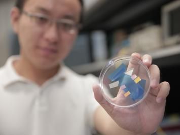
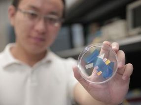
UW-Madison electrical and computer engineering graduate student Zhenyang Xia holds a dish containing photodetector samples. The sample colors vary depending on how they are tuned to absorb a specific light wavelength.
Stephanie Precourt/UW-Madison
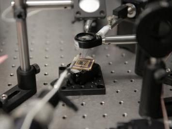
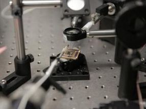
Shrinking photodetectors like this one, created and tested in the laboratory of UW-Madison engineering Professor Zhenqiang (Jack) Ma, help make consumer electronics smaller.
Stephanie Precourt/UW-Madison
Smaller also is better for optoelectronic devices -- like camera sensors or solar cells -- which collect light and convert it to electrical energy. Think, for example, about reducing the size and weight of a series of solar panels, producing a higher-quality photo in low lighting conditions, or even transmitting data more quickly.
However, two major challenges have stood in the way: First, shrinking the size of conventionally used "amorphous" thin-film materials also reduces their quality. And second, when ultrathin materials become too thin, they become almost transparent and actually lose some ability to gather or absorb light.
Now, in a nanoscale photodetector that combines a unique fabrication method and light-trapping structures, a team of engineers from the University of Wisconsin-Madison and the University at Buffalo has overcome both of those obstacles.
The researchers -- electrical engineering professors Zhenqiang (Jack) Ma and Zongfu Yu at UW-Madison and Qiaoqiang Gan at UB -- described their device, a single-crystalline germanium nano-membrane photodetector on a nano-cavity substrate.
"The idea, basically, is you want to use a very thin material to realize the same function of devices in which you need to use a very thick material," says Ma.
The device consists of nano-cavities sandwiched between a top layer of ultrathin single-crystal germanium and a reflecting layer of silver.
"Because of the nano-cavities, the photons are 'recycled' so light absorption is substantially increased -- even in very thin layers of material," says Ma.
Nano-cavities are made up of an orderly series of tiny, interconnected molecules that essentially reflect, or circulate, light. Gan already has shown that his nano-cavity structures increase the amount of light that thin semiconducting materials like germanium can absorb.
However, most germanium thin films begin as germanium in its amorphous form -- meaning the material's atomic arrangement lacks the regular, repeating order of a crystal. That also means its quality isn't sufficient for increasingly smaller optoelectronics applications.
That's where Ma's expertise comes into play. A world expert in semiconductor nano-membrane devices, Ma used a revolutionary membrane-transfer technology that allows him to easily integrate single crystalline semiconducting materials onto a substrate.
The result is a very thin, yet very effective, light-absorbing photodetector -- a building block for the future of optoelectronics.
"It is an enabling technology that allows you to look at a wide variety of optoelectronics that can go to even smaller footprints, smaller sizes," says Yu, who conducted computational analysis of the detectors.
While the researchers demonstrated their advance using a germanium semiconductor, they also can apply their method to other semiconductors.
"And importantly, by tuning the nano-cavity, we can control what wavelength we actually absorb," says Gan. "This will open the way to develop lots of different optoelectronic devices."
Original publication
Xia, Zhenyang and Song, Haomin and Kim, Munho and Zhou, Ming and Chang, Tzu-Hsuan and Liu, Dong and Yin, Xin and Xiong, Kanglin and Mi, Hongyi and Wang, Xudong and Xia, Fengnian and Yu, Zongfu and Ma, Zhenqiang (Jack) and Gan, Qiaoqiang; "Single-crystalline germanium nanomembrane photodetectors on foreign nanocavities"; Science Advances; 2017


Other news from the department science


