Functional fine chemicals for new electronics and electrics: More scope
Advertisement


The IDTechEx report functional materials for Future Electronics: Metals, Inorganic & Organic Compounds, graphene, CNT looks at the new electronics and electrics from the point of view of suppliers of fine chemicals and associated high added value processes. The electrically functional fine chemicals needed most widely for future disruptive electronics and electrics are identified: morphologies including form factors, derivatives, reasons, trends and niche opportunities. This helps the chemicals and materials industries to de-risk their new investments - if one new type of device is unsuccessful, the developed chemicals can be used elsewhere.
That part of the report dealing with inorganic compounds finds that In, Ti, Zn, Al, Ga, Li, Mn, B then Cu will be the most popular anions in compounds with the widest variety of use in the new electronics and electrics but care is needed because there is scope for large volumes of alternatives in premium-priced form if certain device discoveries fulfil their initial promise.
Potential of 2D atomic crystals
For example, following discovery and exploitation of graphene, a host of other 2D atomic crystals are being investigated and electronic, electro-optical and electrical devices made from them. These are mainly inorganic compounds, not carbon allotropes. From Manchester University, Novoselov pointed out in Nature that 2D BN, NbSe2, TaS2, MoS2 and many other options are in the frame. As with graphene, the new 2D materials can be obtained by mechanical or liquid-phase exfoliation of layered materials or CVD growth. Alternatively, start with an existing 2D crystal (like graphene) and use it as atomic scaffolding, modifying it by chemical means. This gave us graphane and fluorographene. The choice of possible 2D crystals is huge, covering a massive range of properties, from the most insulating to the most conductive, from the strongest to the softest, they pointed out.
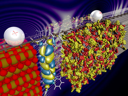
If 2D materials provide a large range of different properties, sandwich structures (made up of two, three, four or more different layers of such materials) can offer even greater scope. These 2D-based heterostructures can be tailored with atomic precision and individual layers of very different character can be combined, so the properties of these structures can be tuned to fit an enormous range of possible applications. The functionality of heterostructure stacks is embedded in the design. The first examples have already started to appear, with vertical tunnelling transistors based on this type of heterostructures having been demonstrated in 2013-4, showing very promising characteristics.
Progress towards 2D optoelectronics
In March 2014, it was announced in Austria that a special type of diode made from a crystalline material whose layers are just three atoms thick has been successfully realized for the first time. The superior properties of such ultra-thin crystals open up previously unimagined possibilities for solar cells, photodiodes and light-emitting diodes, many potentially involving large amounts of new fine chemicals and new manufacturing technology because either very large numbers or areas of devices are needed.
The paper, now published in Nature Nanotechnology, not only documents the actual functionality of a p-n diode made of tungsten diselenide, it also demonstrates its usefulness for numerous applications. These findings, obtained through an Austrian Science Fund FWF project, thus constitute significant progress on the future path to 2D optoelectronics.
Electronic devices require semiconductors. These are usually made from crystalline silicon. The state of the art here is the use of three-dimensional crystals. But these not only combine low flexibility with high weight - they are also expensive to manufacture. Alternative approaches - organic semiconductors and thin-film technologies - result, in turn, in materials with inferior quality and durability. Two-dimensional (2D) crystals - crystalline material layers with a thickness of just one or a few atoms - offer a better chance of success. They can be produced economically on a large scale and are flexible, yet still exhibit all the advantages of crystalline materials. Now a team from the Institute of Photonics at the Vienna University of Technology has succeeded in producing the first diode with a p-n junction from such 2D crystals - thus laying the foundation for radical changes in optoelectronics.
The starting material used for this by the team working with Prof. Thomas Mueller was tungsten diselenide (WSe2). It has one major advantage over graphene, as Prof. Mueller explains: "Tungsten diselenide has a band gap - so electrons require a certain energy to cross over to the conduction band. Graphene cannot easily provide this basic requirement for many electronic components." To ensure that WSe2 was actually present in the form of a 2D layer for the team's further work, it was mechanically "peeled" from three-dimensional crystals in such a way that layers having a thickness of just 0.7 nanometers were created. As Prof. Mueller explains: "We subsequently used complex procedures to check whether we had indeed succeeded in realizing 2D crystals, as only such thin layers exhibit the required properties." Spectroscopic analyses, optical contrast measurements and atomic force microscopy confirmed that the researchers had achieved the desired result. The monolayer WSe2 was then placed between two electrodes and the electrical characteristics were measured. This unambiguously confirmed its function as a p-n diode: it was possible to inject both positive (p, holes) and negative (n, electrons) charges, with current flow exclusively in one direction, as is usual in diodes.
"WSe2 in monolayer crystalline form is theoretically an ideal starting material for p-n diodes and optoelectronics - but no one had ever proven it before. We have now done just that. We measured an efficiency of 0.5 percent in converting light to electrical energy," says Prof. Mueller, explaining the first demonstration worldwide of the photovoltaic characteristics of a 2D crystalline material. The high transparency, at 95%, means it can even be used simultaneously as window glass and as a solar cell, something IDTechEx assesses to have large addressable market, particularly if price competitive and preferably flexible. However, it is also possible to stack several such ultra-thin layers one on top of another to increase the efficiency to as much as 10% but at the expense of transparency. The material's functionality as a photodiode was also proven, achieving a sensitivity one order of magnitude higher than that of graphene. Here is impressive proof that WSe2 possesses superior optoelectronic properties that create new possibilities for solar cells, photodiodes and light-emitting diodes.
Technologies and market forecasts
Another interesting inorganic advance is smart glass, where the new IDTechEx report, Smart Glass 2014-2024: Technologies, Markets, Forecasts finds that the global smart glass market will reach a value of $700 million by 2024.


Other news from the department business & finance


